Accelerating FPGA Development: From Specification to System Validation with IDS-FPGA
Join Agnisys for a technical deep dive into IDS-FPGA, a comprehensive solution that automates the end-to-end FPGA development process, from high-level design specification through RTL generation, system integration, simulation, and hardware/software co-verification.
This webinar features a complete design flow demonstration using a real-world Ethernet Generator and Monitor example, illustrating how IDS-FPGA helps eliminate manual steps, reduce errors, and improve design quality and turnaround time.
This flow is demonstrated using an Ethernet Generator and Monitor design example.
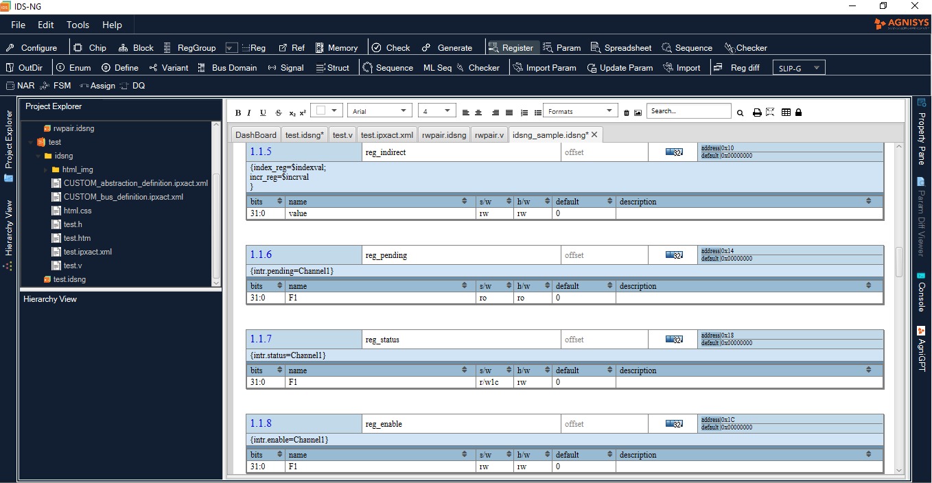
1. Design Specification using our GUI based tool
The process begins with our GUI-based tool used to define hardware architecture at a high level. Designers can configure components such as interfaces, registers, memories, FIFOs, and connectivity. Our GUI based tool generates:
- Synthesizable RTL (Verilog/SystemVerilog)
- Addressable register maps
- Design documentation
- Interface metadata (AXI/APB/AHB, etc.)
2. System Integration with our Integration tool
Our integration tool automates system-level integration. Based on the RTL generated by our GUI-tool, our Integration tool creates:
- Mirror files for software interaction with the register model
- Top-level connection files and interface instantiations
- AXI/APB interconnects
- Module instantiations and hierarchical port wiring
This eliminates the need for manual top-level coding and ensures consistency between design and integration layers.
3. TCL Script Generation for Design Inclusion
The flow generates TCL scripts in the IDS project directory. These scripts are used to:
- Add RTL files and generated components into FPGA projects
- Configure simulation and synthesis flows
- Automate top-level design assembly
These scripts can be integrated with standard FPGA toolchains to streamline and automate the build process.
4. Verification with our Verification and Validation tool
For functional and integration-level validation, the IDS-FPGA flow leverages:
- Our Verification Environment: Generates UVM-based verification environments, including agents, monitors, sequences, and scoreboards.
- Our Validation tool: Produces C-based tests and assertions for early firmware validation and property checking.
This provides full-stack coverage from interface protocol to functional behavior and embedded software access.
5. Integration with FPGA Development Environments
IDS-FPGA supports direct export to popular FPGA design platforms, converting RTL into XML components compatible with system design tools. The process includes:
- Packaging RTL into platform-compatible formats
- Integration with embedded processors (e.g., Nios II)
- TCL-based project setup
- Peripheral and memory-mapped connectivity configuration
6. Hardware/Software Co-Design and Co-Verification
Final validation involves running the generated C tests within a software environment alongside the synthesized RTL.
This step ensures:
- Correctness of register access mechanisms
- Functional correctness of the design in the system context
- Synchronization between hardware and software development teams
The co-verification phase verifies control, data, and status paths while allowing early firmware validation and debugging.
More Visit to explore the complete IDS-FPGA development flow in action. This webinar offers a practical demonstration of how Agnisys tools automate RTL generation, system integration, verification, and hardware/software co-validation. Whether you’re designing or verifying FPGA-based systems, this session will provide valuable insights to streamline your workflow and improve efficiency.