Automating IP and SoC Development
The last month has been busy for all of us at Agnisys, with three important virtual events. As I previewed in my last post, we held our first Agnisys User Group Educational Roundtable (AUGER) on March 18. We had a great event enhanced by lots of interaction with our users. Prior to that, we presented the paper “ML-Based Verification and Regression Automation” and the short workshop “RISC-V Based SoC Design, Verification and Validation in One Hour” at the annual Design and Verification Conference (DVCon) U.S. We also participated for the first time in DVClub Europe, where I discussed “Automating IP and SoC Verification.”
As part of preparing for these events, we took a step back and thought from the top down about the role we are playing in the industry today and the directions we can take in the future. We have expanded our original focus on register automation to encompass specification-driven design, verification, embedded programming, validation, and documentation of IPs and SoCs. This expansion is testament both to our growth as a company and to the many challenges faced by semiconductor development teams. Sheer complexity is the most obvious issue; today’s designs contain billions of gates with thousands of blocks and countless interconnections.
It’s impossible to develop a chip this large without effective reuse. This happens across the industry via standards, across projects using design and verification IP, and across levels, from block to subsystem to full SoC. Of course, there is also new design content in every chip, and hand-writing all the design, verification, and software takes precious time and consumes valuable resources. Tight project schedules demand that code generation be automated wherever possible, which also minimizes manual coding errors and improves code quality.
The challenges are greater in an SoC than a traditional chip because of the combination of hardware and software. The design blocks must be integrated properly, the embedded software controlling these blocks must be merged, and the entire hardware-software system must be validated together. There are also more engineers involved: architecture, hardware design, verification, embedded programming, and system validation teams. A common specification is essential to keep these teams aligned, but that’s easier said than done. There is no standard way to capture specifications, with different teams using different methods. Most use natural language, which is inherently ambiguous and subject to differing interpretations.
Even if a perfect specification somehow exists, change is the only certainty. Issues discovered during implementation and responses to competitive pressures require modifications to every specification many times on every project. Whenever this happens, it causes a waterfall effect. Changes to the hardware design are almost always required, mandating re-verification. In many cases, software revisions are also required, mandating re-validation. End-user documentation must be aligned with the changed specification. If all the updates for the design, verification environment, embedded code, and documentation are made manually, many times per project, the impact is huge.
Specification-driven automation is the only viable solution. Whenever possible, specifications must be captured in an executable format and used to automatically generate code and documentation for all stages in the development process. This is where Agnisys comes in. We provide a wide range of products that support many forms of specification, check for correctness, and then perform the generation steps. As shown in the diagram below, this process has multiple aspects with benefits for multiple teams on the IP or SoC project.
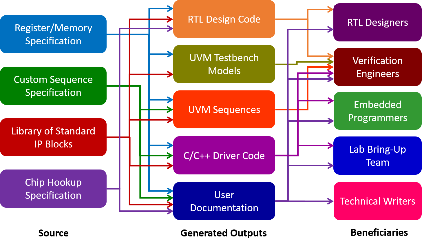
This process has four primary specification inputs:
- The specification for registers and memories is used to generate design RTL code, UVM testbench models and sequences for verification, C/C++ code for drivers and embedded software, and user documentation
- For standard IP blocks, the library generates all the same outputs.
- For non-standard blocks, the specification for custom sequences generates UVM sequences, C/C++ code, and documentation.
- For SoC-level connection of IP and custom blocks, the chip hookup specification generates the top-level RTL design and documentation
This process benefits five primary project teams:
- The hardware designers use the generated RTL code as part of their designs
- The verification team incorporates the generated UVM models and sequences into their testbenches, and may also run the generated C/C++ code for initial validation
- The embedded programmers include the generated C/C++ code in their drivers and other software that communicates directly with the hardware
- The bring-up team runs the drivers and embedded code in the lab as part of full-system hardware-software validation
- The technical writers incorporate the generated documentation into their user manuals
Because of the frequent changes in specifications, this process saves time and resources many times over the course of the project, not just once. It eliminates hand coding, tedious manual updates, introduced errors, and the verification effort to find and fix these errors. Agnisys automates hardware design, software coding, verification, validation, and documentation for many parts of IP and SoC development. To learn more about how this process works, including which products handle which aspects of the flow, please watch our DVCon introductory video.