Count Interrupts Count Interrupts Designs often have a need to count the number of times an interrupt signal occured. An interrupt is a signal generated and sent to the processor by hardware or software indicating that an event needs attention. IDesignSpec has several properties for describing various aspects of the design. These properties can be used together to achieve new functionality! For example, to count the interrupt on the line you can use the counter properties. {counter.sw.wr.enb=regname.fieldname,intr; counter.sw.wr=incr,1} A block is taken with various registers and property is applied on it:

In the above example following properties have been used:

intr.pending=a

This property used to check any pending interrupt on that register. Pending register is originally the Logical And of interrupt source & enable field. Interrupt source can be registered in a flip flop or it can be a signal.

intr.status=a

When interrupt source is asserted or detected for edge it writes 1 to status register. Firmware reads this register to identify active interrupts denoted by value 1 in field and acknowledges/clear the interrupts by writing one to it or reading from it.

intr.enable=a

The enable register enables the interrupts to propagate to CPU by writing one to it. Enable bit corresponding to Status register bit decides whether that interrupt will be allowed to propagate or not. Firmware writes one to bit position where It can be identified using property intr.enable at register or field

And finally, the set of properties {counter.sw.wr.enb=regname.fieldname,intr; counter.sw.wr=incr,1} are used to count the interrupt on that line which has not been cleared .

Here,

counter.sw.wr.enb=regname.fieldname,intr : Used to count the interrupts

counter.sw.wr=incr,1 : Increments the count of interrupts by 1.

Numerous other combinations are possible. You are limited only by your imagination!

Serial Peripheral Interface

The Serial Peripheral Interface bus (SPI) is a synchronous serial communication interface specification used for short distance communication. The SPI bus specifies four logic signals:

  • SCLK: Serial Clock (output from master).
  • MOSI: Master Output Slave Input, or Master Out Slave In (data output from master).
  • MISO: Master Input Slave Output, or Master In Slave Out (data output from slave).
  • SS: Slave Select (often active low, output from master).

SPI with IDS internal signal connections

SPI in IDS

In order to synchronize SPI bus with IDS proprietary bus we will be taking this information from the master through the data line (MOSI). So, for a read or write cycle, first 8 bits will be the IDS instruction set, next 8 bits will be the address of the register to which it wants to communicate and next will be the data bits which depend on the bus width of the proprietary bus.

Regarding the IDS Instruction Set: –


read/write.

For 8-bit instruction set, the maximum value of bus width of proprietary bus will 32 bits.

Implementation

There will be a SPI slave widget which will convert the serial data received from master/user into parallel data or parallel data from IDS RTL into serial, then this data will be received or given to proprietary bus which then communicate with the IDS rtl.

There will be no new property, we just have to instantiate this widget into IDS rtl.

Customer can use this widget just like they are using our other widgets.

Note :- SPI supports only CPOL=0 ,CPHA=0 transfer mode.

Timing Diagrams

Below is an example of a read/write transaction for a 8 bit register having address (8’b00000000).

Write Transaction:-


Read Transaction:-


Summary :

The SPI bus is a synchronous serial communication interface specification used for short distance communication. In order to synchronize SPI bus with IDS proprietary bus, information will be taken from the master/user through the data line (MOSI). So, for a read or write cycle, first 8 bits will be the IDS instruction set, next 8 bits will be the address of the register to which it wants to communicate and next will be the data bits which depend on the bus width of the proprietary bus.


I2C Supported in IDS

IDS now supports the Serial interface via the I2C bus protocol. Various operating modes are implemented.

It contains the I2C-bus data transfer, handshaking and bus arbitration schemes. I2C widget is implemented for 7 bit addressing mode as user will specify the address of the device as slave address. Which will be user specified. 8-bit register address is supported for read and write the data. The I2C widget will take data into I2C format from I2c Master device and converts it to proprietary interface.

I2C0

i2c with IDS internal signal connections

User can easily communicate with IDS serially using I2C master from the host (software) side. There are some initial configurations before starting with I2C: IDS provides a way to configure these initials at the beginning itself. It provides the user with configurable bus select option, I2C then selects device addressing mode and slave address.

The I2C provides an interface between the Master and other devices compliant with Philips Semiconductors Inter-IC bus (I2C-bus) specification version 2.1 and connected by way of an I2C-bus.

Most TI devices (c5000, c6000, OMAP, Davinci, etc.) use the underlying modules.

Supported Bus Features

  • Compatible with Philips I2C Standard. Only two bus lines are required; a serial data line (SDA) and a serial clock line (SCL).
  • Single master operation
  • Software programmable clock frequency, Generally 3 Transmission speeds: Normal, Fast, and High Speed.
  • Clock stretching and wait states generation.
  • Software programmable acknowledge bit.
  • Interrupt or bit polling driven for each byte.
  • Start, Stop, Repeated Start detection.
  • Supports 7 bit with configurable address masking in slave mode.
  • Supports strict I2C reserved rule, Detects general call addresses.
  • Support for IDS compatible byte format transfer for Register address.
  • Bus busy detection.

i2c with IDS internal signal connections

The I2C Widget provides an interface between I2C Slave (A Two wire information) and IDS internal signals. This widget can be used at software side of the IDS and provides a way of introducing serial communication channel for the clients.

FSM Diagram for I2C Widget


A finite state machine for I2C controller

7-bit Slave Address and RD/WR bit Format

After the START condition (S), a slave address is sent. This address is seven bits long followed by an eighth bit which is a data direction bit (R/W) — a ‘zero’ indicates a transmission (WRITE), a ‘one’ indicates a request for data (READ).

A data transfer is always terminated by a STOP condition (P) generated by the master. However, if a master still wishes to communicate on the bus, it can generate a repeated START condition (Sr) and address another slave without first generating a STOP condition. Various combinations of read/write formats are then possible within such a transfer.


A complete Data Transmission by I2C

Configurable Addressing

IDS provide a facility to configure 7-bit addressing of a particular device before start generation of I2C Interface with IDS. This addressing follow all the rules and regulations complaint with Philips Semiconductors Inter-IC bus (I2C-bus) specification version 2.1.

8-bit of Register Address:

After the slave address is acknowledged, user needs to send a byte that is a specified IDS register address which is byte addressable by the increment of four bytes for each register.

If there is a memory specified, this controller will take care of an appropriate address calculation or an offset value compatible with IDS requirements.

Because the default address of an IDS registers is 32 bit, widget will split this address into separate bytes which are followed by one after the other covering the full register by using repeated Start logic.

Summary

In addition to I2C we have also supported the SPI bus. Please contact support for access to these widgets and latest executable with the new support.


HDL PATH for Gate Level Simulation

In UVM, the register abstraction layer describes the register and memory behavior of the Design Under Test (DUT). An “hdl_path” is specified for the RTL storage of the registers. When the Gate level simulation is performed, the corresponding hdl_path properties need to be added.

We can read/write the register or memory with two methods:

  1. Front door access: It completes read/write operation by bus and consumes clock cycles.

  2. Back door access: It completes read/write operation by back door access i.e. simulator database and operation completes in zero time. This method uses ‘hdl_path’ property.

IDS supports the use of front and back door access methods to read/write the register or memory data.

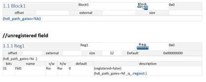
The property ‘hdl_path_gates’ is supported at chip, block, reggroup, register, and field level in the same way as the property ‘hdl_path’. Both properties can be simultaneously added to the model. The value of hdl_path_gates can be an explicit string, or a string pattern.

It has zero time simulation for read and write through peek() and poke() respectively. Therefore, it increases the efficiency.

When the synthesis of RTL is performed, the gate level netlist is completely different with different storage elements and different instance names. Fortunately, these instance names created by the synthesis tool have some order (usually) so that we can provide a pattern to the hdl_path_gate property which will refer to the equivalent storage in the RTL.

  1. How to add multiple hdl_path_gates?

hdl_path_gates=”ff1.q, ff2.q”

If a field is split into multiple gate level storage elements, one can specify a list of elements.

  1. Automatic generation of hdl_path_gates from hdl_path using patterns

Hdl_path = reg1_FF_q

Hdl_path_gates= %r_%f_q

Where %r and %f are the name of the register and field respectively.

The above can be specified in a more generic way by using patterns for block (%b), register (%r) and field (%f) as shown below.

Here %M= value of field MSB,   %L= value of field LSB
%c =Chip name,       %b=Block name,      %s=Reg Group name ,
%r=Register name, %f=Field name, %m=Memory name
All small letter operator can add comma separated value before (prefix) and after(Suffix) .
As: %r . will generate as Reg1.

Generated UVM code:

add_hdl_path(“Block1″,”GATES”);

Reg1.clear_hdl_path();
Reg1.add_hdl_path_slice(“Reg1.Fld1_q_.regout”, 31, 1, ,”GATES”);
Reg2.clear_hdl_path();
Reg2.add_hdl_path_slice(“Reg2mode_q_31_.regout”, 31, 1, ,”GATES”);
Reg2.add_hdl_path_slice(“Reg2Mode1_q_20_.regout”, 20, 1, ,”GATES”);
Reg2.add_hdl_path_slice(“Reg2Mode1_q_19_.regout”, 19, 1, ,”GATES”);
Reg2.add_hdl_path_slice(“Reg2Mode1_q_18_.regout”, 18, 1, ,”GATES”);
Reg2.add_hdl_path_slice(“Reg2Mode1_q_15_.regout”, 15, 1, ,”GATES”);
Reg2.add_hdl_path_slice(“Reg2Mode1_q_12_.regout”, 12, 1, ,”GATES”);
Reg2.add_hdl_path_slice(“Reg2Mode1_q_11_.regout”, 11, 1, ,”GATES”);
Reg2.add_hdl_path_slice(“Reg2Mode2_q_10_.regout”, 10, 1, ,”GATES”);
Reg2.add_hdl_path_slice(“Reg2Mode2_q_9_.regout”, 9, 1, ,”GATES”);
Reg2.add_hdl_path_slice(“Reg2Mode2_q_8_.regout”, 8, 1, ,”GATES”);
Reg2.add_hdl_path_slice(“Reg2Mode2_q_7_.regout”, 7, 1, ,”GATES”);
Reg2.add_hdl_path_slice(“Reg2Mode2_q_6_.regout”, 6, 1, ,”GATES”);
Reg2.add_hdl_path_slice(“Reg2Mode2_q_5_.regout”, 5, 1, ,”GATES”);

Mem1.clear_hdl_path();
Mem1.add_hdl_path_slice(“Mem1”, 0, 32, , “GATES”);

Usage Models

set_hdl_path_root( ,“GATES”) ;
set_hdl_path_root( ,“RTL”);

Testing process:-

We are using ARV environment for testing.
The top level hdl path can also be defined in the uvm environment class in the arv directory

“ids output directory -> arv -> env -> env.svh” as:

begin

string hdl_root=” wrapper.u_dig_top.u_controller_bist_top.u_controller_top.u_ids_top.u_reg_map”;
void'($value$plusargs(“ROOT_HDL_PATH=%s”,hdl_root));
cfg.model.set_hdl_path_root(hdl_root, “GATES”);
cfg.model.set_hdsssl_path_root(hdl_root, “RTL”);
void'(cfg.model.set_coverage(UVM_CVR_ALL));

end

The testing sequence file “ids output directory -> arv -> sequences -> arv_seq_lib.sv” contains library of register sequences to test the DUT. The design abstraction models (“RTL” or “GATES”) is specified in the register peek/poke methods used for backdoor access.

Examples:

rg.poke(status, write_val .parent(this),.kind(“GATES”));
rg.peek(status, read_val, .parent(this),.kind(“GATES”));

Notes:
The functionality is same as the property hdl_path, only enhanced.

Parameterization in IDS

In IDesignSpec parameters are constants that can be changed from the simulation command line. Typically, parameters are used for constants like number of clients, number of ports, inclusion/exclusion of blocks etc.

A parameter can have a value as a literal constant or another parameter or an arithmetic expression with constants and other parameters.

Parameters give us huge re-usability of the codes. It means we can use same module/code various times in a big design and each time it’s configuration can be different.

In IDesignSpec parameters can be passed to a module using three different methods: –

  1. Simple parameter passing
  2. Passing array via parameter.
  3. Bit slicing of parameters.

Property associated with SystemVerilog Parameter. Property “sv_param” for SV Header which converts the `define to the parameter inside the package.

1. Simple Parameter passing: –

In IDS, user is now able to specify parameters and defines in the define table typically at the top of the document and use these as macros to assign values to all properties.

Parameter Creation

  • Parameter’s name should start with ‘$’
  • Value of the parameter can be static or based on an expression. Both String and numeric expressions are allowed.

Rules for defining ‘parameters’

  • Parameter’s value can depend on already specified parameters.

Following example shows parameter and define creation in IDS-

IDSWord: –

In IDSWord, add a define template to parameters to the design spec.

Verilog Code: –

module block_name_ids (

Reg1_enb,
Reg1_enb,
Reg1_Fld1_in,
. . .
. .
parameter Chip_off = ‘h1000 ; //
parameter Block_off = ‘h100 ; //
parameter Reg1_off = ‘h10 ; //
parameter Reg_group1_off = ‘h400 ; //
parameter Reg1_1_off = ‘h40 ; //
parameter Reg_def1 = ‘h70 ; //
parameter Reg_def2 = ‘h17 ; //
parameter Register_width = 16 ; //
parameter Num_lanes = 16 ; //
parameter NUM_CHANNELS = 80 ; //

parameter Reg_group1_count = Num_lanes;
parameter Reg_group1_address_width = 5;

parameter Reg1_count = NUM_CHANNELS % Register_width == 0 ?
NUM_CHANNELS/Register_width : NUM_CHANNELS/Register_width + 1;
parameter Reg1_address_width = 11;
. . .
. .

generate
genvar Reg1_i;
for( Reg1_i = 0; Reg1_i < Reg1_count; Reg1_i = Reg1_i + 1)
begin : Reg1_gen
. . .
. .

assign Reg1_offset[Reg1_i] = block_offset+(Reg1_off) * 1 + Reg1_i * ‘h4;
assign Reg1_decode[Reg1_i] = (address[Reg1_address_width-1 : 0] ===Reg1_offset[Reg1_i]) ? 1’b1 : 1’b0;

always @(posedge clk)
begin
if(!reset_l)
begin
Reg1_Fld1_q[Reg1_i] <= Reg_def1 + 4;
end
. . .
. .

if(!reset_l)
begin
Reg1_Fld2_q[Reg1_i] <= Reg_def2 *2;
end
. . .
. .

end //Reg1_gen
endgenerate

generate
genvar Reg_group1_i;
for( Reg_group1_i = 0;
Reg_group1_i < Reg_group1_count;
Reg_group1_i = Reg_group1_i + 1)
begin : Reg_group1_gen
. . .
. .
assign Reg_group1_Reg1_1_offset[Reg_group1_i] = block_offset+(Reg_group1_off) * 1 + Reg_group1_i * ‘h44 + (Reg1_1_off) * 1;
assign Reg_group1_Reg1_1_decode[Reg_group1_i] = (address[Reg_group1_address_width-1 : 0] ===Reg_group1_Reg1_1_offset[Reg_group1_i]) ? 1’b1 : 1’b0;
always @(posedge clk)
begin

if(!reset_l)
begin
Reg_group1_Reg1_1_Fld1_q[Reg_group1_i] <= Reg_def1 << 2;
end
. . .
. .
if(!reset_l)
begin
Reg_group1_Reg1_1_Fld2_q[Reg_group1_i] <= Reg_def2 >>1;
end
. . .
. .

   end //Reg_group1_gen
endgenerate
.          .         .
endmodule

2. Passing array via parameter: –

In IDesignSpec user can pass array using parameter for example:

The case below is passing unique parameters to repeated blocks. User can imagine the parameterized value something like an Interface ID.

We are instancing a block a parameterizable amount of times. The block has a register that is like an interface ID register, requiring unique values per instance.

Here, each block will use the default value, resulting in all interface ID’s having the same value.

We conclude that we could have the reset value of the interface ID register be controlled via a parameter, and when it is instanced in a repeat block, each repeat would get a unique value from the array (e.g. repeat index 0 gets parameter index 0, repeat index 1 gets parameter index 1 (if exists))

In the following example parameter is defined in 2-D format which is used in reg_name template later: The parameters are defined in the define table in the following manner:-


Where $P1= name of the parameter [32] = is the width of the parameter [4] = is the depth of the parameter {0,1,2,3,4} = are the value of of the parameter

Below is the representation of how the parameters are used in a register:-

Where the parameter name is given in the default value of the field and repeat property has been defined on the register with repeat value equal to the depth of the parameter.

Verilog Code: –

.          .           .
.          .
parameter Block1_ids_offset = ‘h14;
parameter reg [7:0] P1 [4:0] = ‘{1,2,3,4,6} ; //
parameter [3:0] p2 = 9 ; //
parameter addr_width = 6; parameter bus_width = 32;
.           .           .            .
.           .
generate

genvar section__i;
for( section__i = 0; section__i < section__count; section__i = section__i + 1)
begin : section__gen

.            .          .            .
.            .

always @(posedge clk)

begin
if (!reset_l)
begin
section__F1_q[section__i] <= P1[section__i];
end

.             .          .
.             .

3. Bit Slicing in Parameter: –

There is a way to specify the width of a parameter in IDesignSpec, and there is a way to create a parameter by bit-slicing an existing parameter in IDesignSpec.

like: –
$param1[24] = 0xABCDEF
$param2[8] = param1[23:16]
$param3[8] = param1[15:8]
$param4[8] = param1[7:0]

The parameters are defined in the define table in the following manner:-

Where,

$param1, $param2, $param3, $param4= name of the parameter

[32]= is the width of the parameter
0xABCDEF = is the value of the first parameter
“$param1[23:16]” = where $param2 is assigned the [23:16] values of $param1

These values can later be used in the register fields by declaring them in the register field in the default value part:

Here, the field is assigned the value of the parameter.

Verilog Code: –

.           .           .           .
.           .
parameter [31:0] param1 = ‘hABCDEF ; //
parameter [7:0] param2 = param1[23:16] ; //
parameter [7:0] param3 = param1[15:8] ; //
parameter [7:0] param4 = param1[7:0] ; //
.           .           .           .
.           .
always @(posedge clk)
begin
if (!reset_l)
begin

           Section1_f1_F1_q <= param2;
end

.           .           .           .
.           .

Property- sv_param: –

The property sv_param is applied on the top-level module for SV haeader outputs. It converts the `define to the parameter inside the package.

Below is the example for the same:

SV Header Output: –

package block_name_header_pkg; parameter BLOCK_NAME_ADDR = ‘h00;
parameter BLOCK_NAME_SIZE = ‘h90;
parameter BLOCK_NAME_MEMORY_NAME_ADDR = ‘h00;
parameter BLOCK_NAME_MEMORY_NAME_SIZE = ‘h4;
parameter BLOCK_NAME_MEMORY_NAME_DEPTH = 32;
parameter BLOCK_NAME_MEMORY_NAME_MASK = ‘hFFFFFFFF;
parameter BLOCK_NAME_REG_GROUP_NAME_ADDR = ‘h80;
parameter BLOCK_NAME_REG_GROUP_NAME_SIZE = ‘h8;
parameter BLOCK_NAME_REG_GROUP_NAME_REPEAT = 2;
parameter BLOCK_NAME_REG_GROUP_NAME_REG_NAME_ADDR = ‘h80;
parameter BLOCK_NAME_REG_GROUP_NAME_REG_NAME_DEFAULT = ‘h00000000;
parameter BLOCK_NAME_REG_GROUP_NAME_REG_NAME_F1_MSB = 31;
parameter BLOCK_NAME_REG_GROUP_NAME_REG_NAME_F1_LSB = 0;
.             .              .             .
.             .              .
typedef struct packed {
logic [31:0][31:0] memory_name; block_name_reg_group_name[2] reg_group_name;
}  block_name;

endpackage

Summary:

This article has shown how parameters are handled in IDesignSpec. Parameter arrays have also been supported. These make a very generic specification for IP/SoC. It goes to show the versatility of IDesignSpec.

Scroll to Top