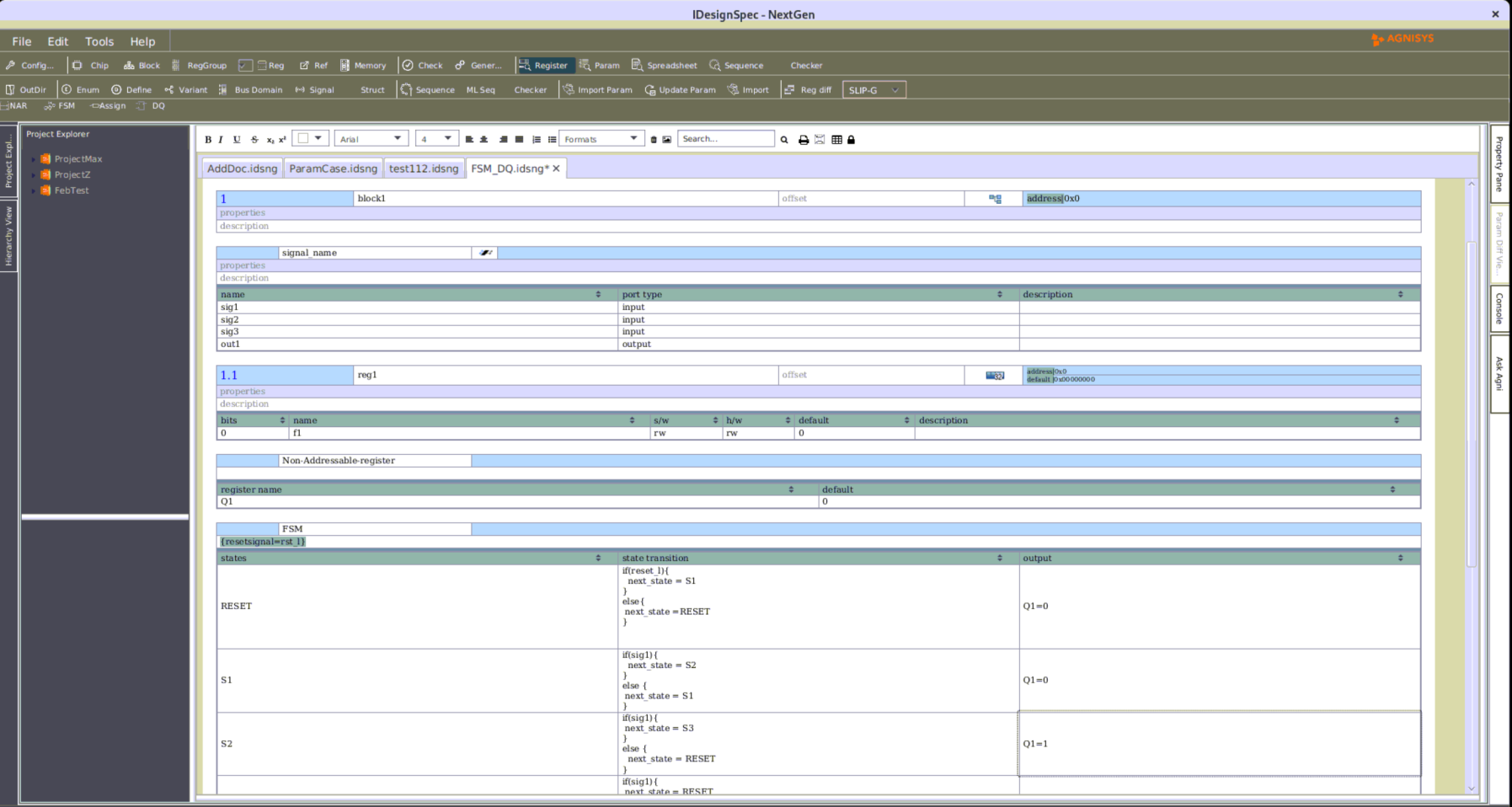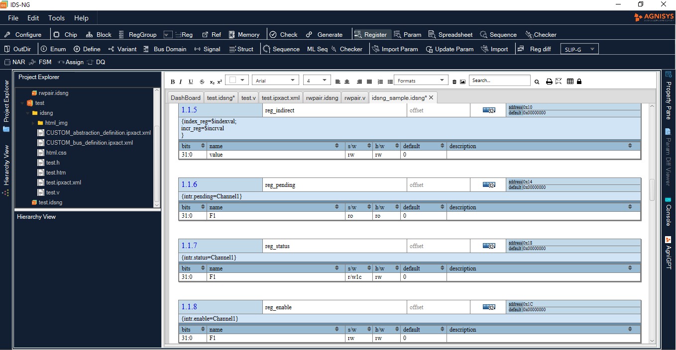
In the webinar titled “AI Chip Design Using Agnisys”, we explored how advanced techniques like systolic arrays, parallel processing, and domain-specific accelerators are reshaping AI chip architectures for speed and energy efficiency. The session highlighted how Agnisys tools, such as IDesignSpec (IDS), automate RTL generation and streamline the design-to-implementation process, minimizing errors and accelerating time-to-market. Attendees gained insights into leveraging neuromorphic chips, 3D stacking, and edge-specific processors to address AI use cases in IoT, robotics, and beyond.
eBook: How Agnisys Eliminates Redundancies in Semiconductor Design, Verification, and Validation
Overcoming the weaknesses of traditional natural language specifications requires writing the specifications in a precise format rather than natural language, and making this format executable so that tools can generate as many files as possible for the design, verification, programming, validation, and documentation teams. Such a solution is available today.
Recent Blog Articles
Verification of modern IP and SoC designs presents several challenges. Specifications are often interpreted differently across teams, such as design...
Agnisys delivers advanced automation solutions that address some of the most complex challenges in chip development, from IP to...
If you’ve worked with Zephyr RTOS, you already know that devicetree files are a core part of how hardware...


