Reliving Your Childhood Joy while Assembling SoCs
As kids, many engineers enjoyed toys that involved assembling complex designs from simple elements. Whether it was wooden blocks, LEGO bricks, ERECTOR sets, or Tinkertoy pieces, I’ll bet that you played with something of this sort. Maybe you still do! But manually assembling all the pieces of a modern semiconductor design into a complete system on chip (SoC) is not nearly as fun as these toys. In this post, I’ll offer a way to make this process much easier, less tedious, and correct by design.
Challenges of the Chip Business
SoC assembly is just one phase in the long and involved process of developing your SoC. I think it’s important to outline the context of this development before discussing assembly and packaging in particular. At the highest level, SoC suppliers face enormous market pressure. Advanced applications such as AI, high-performance computing (HPC), and autonomous vehicles demand maximum performance from the chips performing the key computations.
However, it’s not just about pure speed. The design of a modern SoC is highly complex, with many IP blocks integrated into a deep hierarchy of subsystems interconnected by buses and network-on-chip (NOC) links. Large on-chip memories and a wide array of external interfaces must also be connected.
The sheer size is also daunting: an SoC may contain hundreds of millions—even billions—of gates. It is no surprise that your development takes months or years and requires large engineering teams.
Unfortunately, project schedules are rarely flexible. The highly competitive nature of the leading applications means that time to market is critical. Late product introduction may never generate the sales needed to cover the development costs, let alone earn some profit. The accelerated pace of industries such as AI means that most chips have a fairly short shelf life. This compresses schedules even more, while reducing your likelihood of making money.
You face constant pressure to reduce both the cost of the manufactured chip and the cost of the development process. Reusing parts of your existing designs, acquiring design and verification IP from multiple sources, and automatically generating design and verification code are all solutions being used today to produce bigger and more complex chips with smaller teams in less time. The themes of reuse and automation appear throughout a modern SoC development process.
Why SoC Assembly Is Not a Game
When people talk about a better development methodology with increased return on investment (ROI), they often focus on the internals of the chip design. Many of the IP blocks acquired or auto-generated are either fairly small or clearly delineated subsystems such as processors. It seems that people often dismiss the fact that all those bits and pieces have to be interconnected to form a complete SoC. They may assume that this is a tedious but straightforward process.
This is not the case. Assembling your SoC is nothing like playing with building-block toys. For one thing, the sheer number of interconnections is staggering. A typical SoC with 500 IP blocks and an average of 300 ports per block results in roughly 150,000 ports that must be connected. On a large SoC, this number may balloon to hundreds of thousands. Clearly, trying to make all these connections by hand would tie up your valuable designers and prolong your project schedule.
Manual assembly is error-prone as well as resource-intensive. Many ports, signals, and buses have very similar names. Typos are inevitable, and they often connect the design incorrectly but in a manner that will compile without errors. Finding and fixing these typos as you debug failing verification tests is highly inefficient. Some SoC teams specify the desired interconnections in spreadsheets and use scripts to generate the register-transfer-level (RTL) code for the interconnects.
Simple automation helps a bit, but it is not enough. A complete chip assembly solution must:
- Work at every level of hierarchy, all way up to the complete SoC
- Interconnect signals that pass up and down through levels of hierarchy
- Generate bus “widgets” such as bridges, converters, aggregators, and crossbars
- Rerun quickly and automatically as your design evolves throughout the project
- Modify the hierarchy to reflect any changes made by place-and-route (P&R) tools
Agnisys Is Here to Help
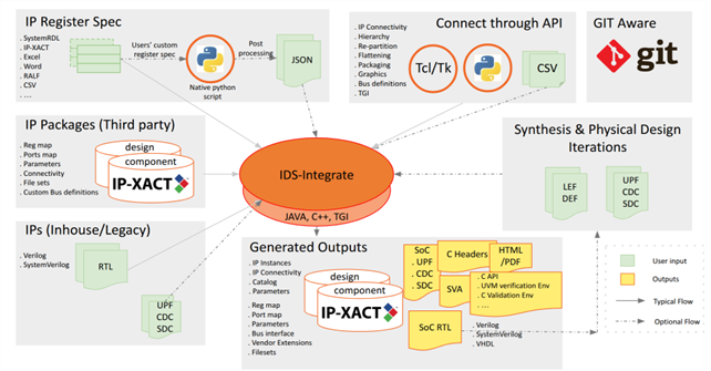
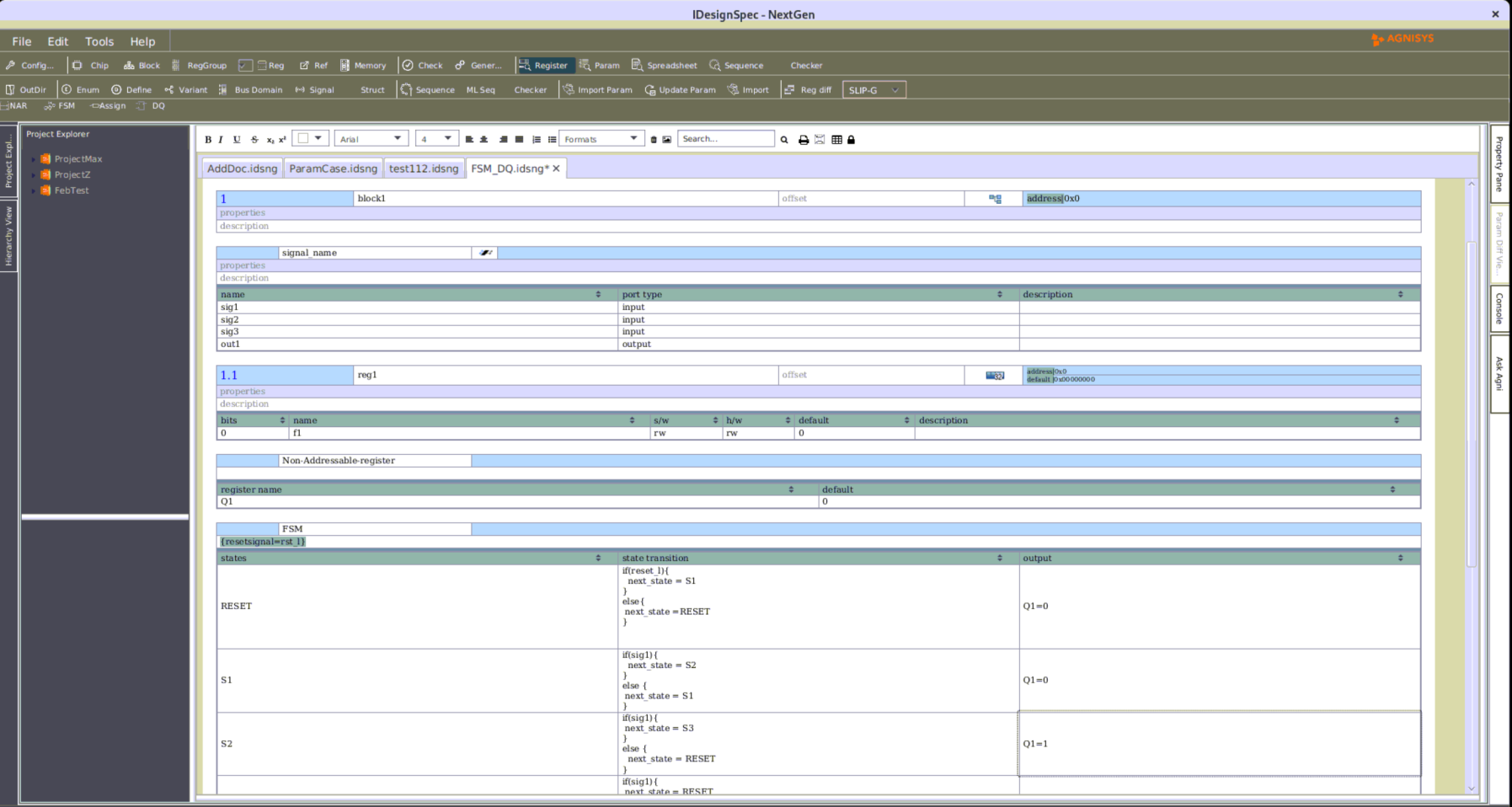
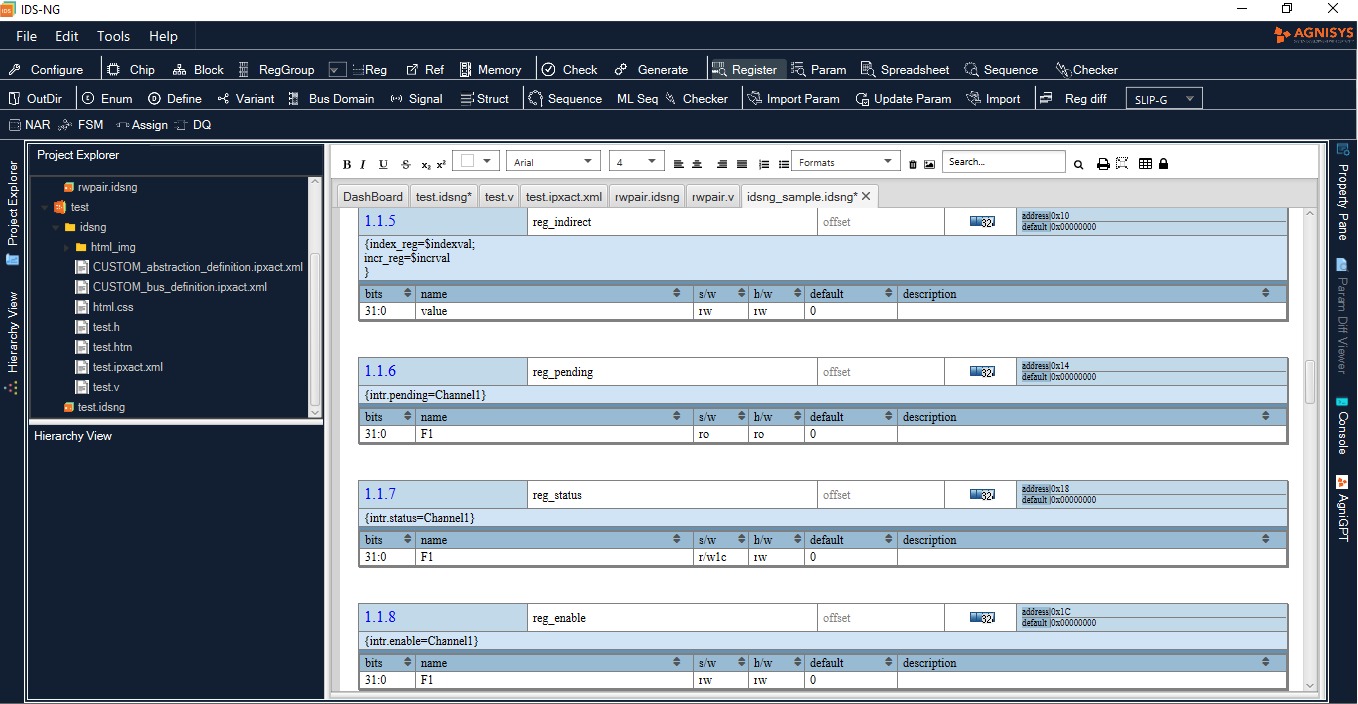
I’ve never seen a rule-based chip assembly “solution” that meets all these requirements. Solving the problem in a big way requires a dedicated tool integrated with all the other automated aspects of your chip design, verification, programming, validation, and documentation flow. As you know, our IDesignSpec™ (IDS) Suite provides specification automation for IP and SoC development. When it comes to chip assembly tasks, our IDS-Integrate™ is a true solution.
A few months back, I discussed IDS-Integrate in considerable detail. I suggest reading that post if you’d like to learn more. I will note here that we satisfy all the requirements I listed above. We generate interconnect RTL code, including bus widgets and interfaces from our Silicon IP Portfolio, for all levels of your hierarchy from a simple but powerful specification format. You can use wildcards so that you don’t have to specify every individual desired connection manually.
As I noted in my previous post, we’ve recently added support in IDS-Integrate for four important standard formats, Unified Power Format (UPF) for power intent, synthesis design constraint (SDC) files, and Library Exchange Format (LEF) and Design Exchange Format (DEF) for post-layout files. We are seeing a lot of interest in this solution, and we will continue to evolve it and add new features as we work with more and more users.
Conclusion
As SoC developers, you and your team face daunting challenges in many parts of your development flow. Our IDesignSpec Suite helps you in many ways, with IDS-Integrate focused on chip assembly. In my next blog post, I’m going to show you some concrete examples of how you can use this tool to build up your SoC in an automated manner that’s correct by construction. In the meantime, please contact us if you’d like to learn more or try out our solutions.


