The Future of Chip Design: Key Trends, Challenges and Innovations in Semiconductors
Semiconductor development is one of the most dynamic industries in history. Change is constant, stemming from evolution in underlying technologies and architecture, punctuated by the occasional revolution, such as the recent focus on AI. For this post, I’m focusing on five key aspects of change in chip design that we are seeing widely in our user base. If you’re facing challenges related to these trends, I’ll let you know how we can help.
AI Is Everywhere
You can’t pick up a newspaper (literally or digitally) these days without seeing AI in the headlines. The rapid increase in capabilities and the potential for the future are astounding. Even if your only interaction with AI is getting more focused search results, you can appreciate how much has changed so quickly. As engineers, we understand more about the hardware and software technology that makes the capabilities of AI possible, and these are impressive as well.
With AI affecting almost every aspect of our lives, it is not surprising that so many chips contain dedicated hardware to make AI algorithms run faster and better. Graphics processing units (GPUs) have turned out to be very good at AI as well as image rendering, and there are AI accelerators such as transformers in use as well. I’ve written several blog posts that discuss the impact of AI chips on the chip development process.
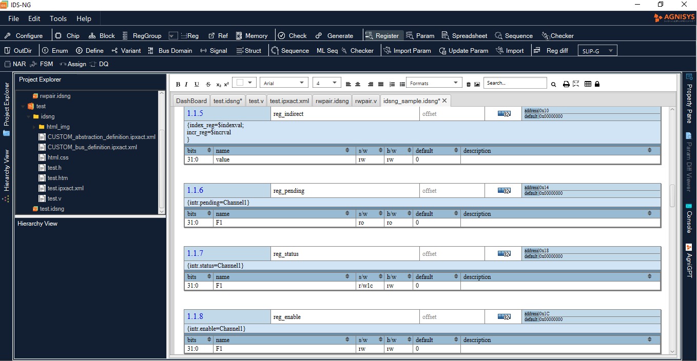
AI applications require massive parallelism, large amounts of fast memory, high-speed communication channels, and flexibility in settings such as weights, parameters, and hyperparameters. These settings cannot be fixed at design time; they must be adaptive to the data being processed. Setting these values on the fly is possible with programmable control and status registers (CSRs), and we provide the industry’s best solution for register design, verification, programming, validation, and documentation.
Flexibility Is Essential
Settings for AI models are just one example of required flexibility and adaptability in modern chips. There are many applications in which startup configurations must be flexible and on-the-fly changes to settings are required. For example, some communication protocols have a training phase in which settings are adjusted to get the best possible performance given the connected devices and the environment in which they operate.
As another example, many chips are designed for multiple applications. Of course, you can’t change the hardware since it’s fixed. But you can program the hardware to behave differently depending upon the application. Again, CSRs are an ideal way to provide this flexibility. The chip datasheet might specify very different initial values depending on the application. As with AI, some of these values might change over time in response to feedback on power, performance, or required functionality.
Our IDesignSpec™ Suite of specification automation products gives you complete control over your CSRs. IDesignSpec GDI and IDS-Batch™ CLI generate register-transfer-level (RTL) designs, C/C++ headers, and documentation for your CSRs. IDS-Verify™ generates Universal Verification Methodology (UVM) compliant tests and testbenches. Finally, IDS-Validate™ generates C/C++ code to program the registers as well as hardware-software validation environments.
Heterogeneous Processors Are Certain
A system on chip (SoC) is often defined as a semiconductor device containing at least one embedded processor. The chip’s functionality is provided by the combination of hardware and software, as would be the case in a multi-chip system. One key aspect of the architecture phase of development is determining which functions will reside in hardware and which will be implemented in software. Trying “what if” scenarios for different partitions is a critical part of the process.
Today’s SoCs are highly unlikely to contain a single processor with a single core. Most processors have multiple cores, and different processors are used for different functions. SoCs may have a heterogenous mix of x86, ARM, and RISC-V cores, GPUs, AI accelerators, and more. Moving functionality around can involve a lot of RTL and software re-coding, and often has ripple effects on the CSRs as well.
We can’t magically re-code your proprietary algorithms, but we can automate your changes to the CSRs. You can re-generate your register design at any time, along with the tests and environments needed to verify and validate it. Since we also generate the C/C++ code to program and access your registers, you have full flexibility. If you add CSRs, simply re-run IDS-Validate to generate new register C/C++ and incorporate it into your drivers, embedded code, or other low-level software.
Chips Are Going Vertical
As you can imagine, a chip with multiple processors and accelerators, plus lots of memory, can be huge. Moore’s Law has slowed, meaning that migrating to new, smaller process nodes may not be possible as frequently as designers would like. Chip sizes are stressing the reticle limits in fabrication, and very large dies are likely to have lower yield than smaller devices. For all these reasons, chip designers are adopting 2.5D and 3D IC configurations.
Multi-die packages offer several advantages, including leveraging existing dies and using dies from different nodes or processes that can’t be combined into a monolithic chip. For 3D devices, inter-die propagation delays are shorter vertically than horizontally. However, the architecture phase gets more complicated. The “what if” scenarios must cover not just the partition between hardware and software, but also the partition of the hardware across multiple dies.
We have a solution here as well: IDS-Integrate™, which automatically connects your design blocks together and generates the top-level RTL code. If you moved a function from one die to another, you simply update the configuration files for the two dies and then re-generate both top-level designs. It is not uncommon to make changes to the design hierarchy even after RTL coding is underway, and we can lessen the impact on you for 2D, 2.5D, and 3D chips.
Markets Demand Portfolios
All of what I’ve discussed so far can help you create one SoC with less effort, in a shorter time, and with lower risk. However, most chips are not one-time stand-alone products. Many SoCs are part of a product portfolio with offerings tailored for different price points or different markets. The number and types of processors may vary, or the amount of embedded memory. A chip for natural language processing (NLP) may have hardware transformers, but one for other AI applications may not.
What this means is that SoC developers want to be able to rapidly create new variations of their designs in response to market trends. You can’t afford to spend a lot of time and resources on each variation. This is another benefit of 3D chips, since you may be able to reconfigure the mix of dies without fabricating any new dies at all, or perhaps limit their changes to just one of the dies. As I noted earlier, we make this process much easier.
Our specification automation solutions help you produce new chips rapidly regardless of how many dies are involved or how they are combined. Modifying your CSRs, rearranging your design blocks, or choosing different blocks from our silicon IP portfolio requires almost no work at all on your side. We automatically generate all new design, verification, programming, validation, and documentation required to reflect your changes.
Summary
The five trends I mentioned in this post are closely related. AI demands flexibility, product portfolios have differing processor needs and may require 3D designs, and so on. You may very well be facing some or all of these challenges on your own chip projects. Please keep in mind all the ways that we can help you, as I’ve outlined above, and give us a call. You’ll be glad that you chose us as your partner.