Automatic Handling of Register Clock Domain Crossings
Register-transfer-level (RTL) code, formal analysis, RTL simulation, and logic synthesis have all raised the abstraction level of electronic design and verification. Today’s designers operate very differently than their predecessors who drew circuit-level schematics and ran only SPICE. However, underneath all this abstraction the physical properties of electronic devices remain unchanged, and these must be considered during design. Metastability is a common issue in clock domain crossings when signals cross between asynchronously clocked flip-flops.
The most common example of metastability happens when the output value of a flip-flop on the sending clock changes during the setup and hold time of the clock for the receiving flip-flop. The output of the flip-flop on the receiving clock can take on an indeterminate value that requires some time to settle to a one or zero. If the output of the receiving flip-flop is used immediately, an invalid value may be fed into the downstream logic and produce incorrect results. Unfortunately, there is no way to design a flip-flop that does not have a risk of metastability.
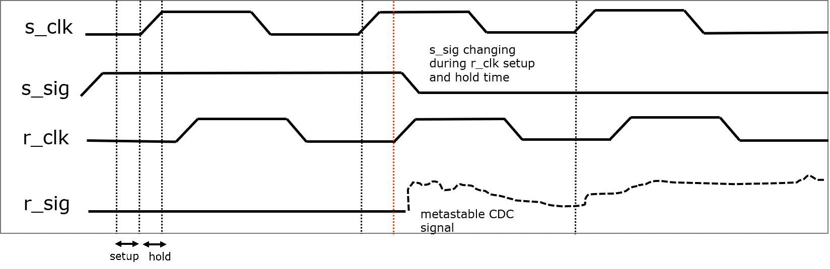
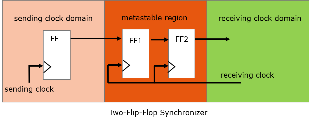
The most common way to handle the metastability problem is to use a synchronizer consisting of two flip-flops on the receiving clock. The aim is for signal stability before the second flip-flop’s output is used by downstream logic. Theoretically, the output from the first flip-flop is still sufficiently metastable when it is clocked into the second flip-flop to cause problems. However, a mean time between failures (MTBF) calculation typically shows a high probability that the metastability will settle before the second flip-flop is clocked and the signal is used.
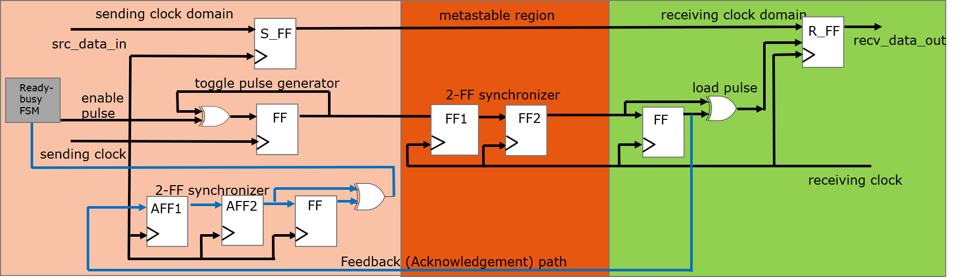
This approach works well for control signals, but it’s insufficient for multi-bit signals such as data buses. Different bits may have different delays due to logic and routing so that they arrive at the receiving flip-flops at different times. An inconsistent data value can be clocked in and used by downstream logic. There are a few ways of addressing this issue, but perhaps the most sophisticated is the handshake synchronizer. This approach establishes a multi-cycle path (MCP) for the data bits so the outputs of the sending flip-flops are held stable long enough that they will not be changing when the values are clocked into the receiving flip-flop. Thus, there is no risk of metastability.
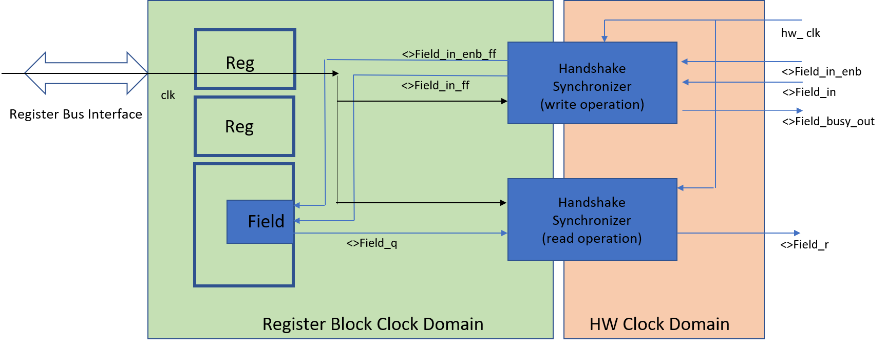
Control and status registers (CSRs) are one part of many designs where asynchronous clocks are often used and metastability is a genuine problem. Most register blocks have a “software” interface on the system bus from which programs running on host systems or embedded processors can write or read the registers. OS boot routines set registers to initial values, and code like ISR and applications read/write registers. Register blocks are usually in the system bus clock domain.
Register blocks also have a “hardware” interface from which the rest of the design can read or write the registers. Hardware operation relies on control and configuration register settings, making the read path crucial. Both the read and write capabilities are vital when registering bits or fields used for handshaking between the hardware and software. Data can also be exchanged using registers. Since the hardware is almost always on a different clock than the system bus, there is a CDC that must be handled properly.
As the industry leader in the automation of register design and verification, Agnisys provides a push-button solution for CDC crossings related to register blocks. IDesignSpec™ (IDS) helps IP/SoC architects and engineers create an executable specification for registers and automatically generate outputs for software and hardware teams. Supported input formats include Microsoft Word and Excel, SystemRDL, and IP-XACT. IDS generates a UVM verification model complete with constraints and coverage, and customizable documentation in such file formats as Word, PDF, and HTML.
Most importantly, IDS automatically generates the RTL code for the register design (in VHDL, Verilog, SystemVerilog, or SystemC) plus a bus slave and decode logic specific to the system bus protocol (AHB, APB, AXI, AXI-Lite, TileLink, or proprietary). If registers differ from the system bus clock domain, IDS generates synchronization logic RTL and formal CDC verification assertions Agnisys has enhanced SystemRDL 2.0 so the designers can specify their desired synchronization method in the register specification.
IDS offers other synchronization options, including two-level flip-flops and mux synchronizers. It can also handle cases where the register block is in its clock domain distinct from the system bus and the rest of the hardware design. This level of automation provides great benefits to designers, who do not have to worry about CDCs at all and provides help for the verification team as well. Agnisys and IDesignSpec, with proven records firming support, is vital for success in asynchronous clock domain designs.
To learn much more about CDCs and the CDC support within IDE, please view our recent webinar.