Custom IP Design and AI-Based Verification
Introduction
Engineers have consistently strived to expedite ASIC development. Our latest endeavor at Agnisys introduces automation that captures specifications in a high-level “template” format and generates all requisite downstream assets.
The automation of addressable registers is a well-established practice in the industry, with both open-source and commercial tools readily available. Upon capturing the register specifications, designers traditionally embark on crafting a synthesizable glue logic layer to enable the intended functionality using these addressable hardware registers. This process often necessitates the use of various design constructs, and the manual work involved is susceptible to errors, requiring frequent revisions.
Hence, there arises a pressing need for an automation technique to alleviate the manual labor associated with glue logic creation. The Agnisys IDesignSpec (IDS) family presents a comprehensive solution for capturing register specifications. By employing the approach outlined in this specification, users can seamlessly generate design functionality (glue logic) using predefined templates. This streamlined process not only augments the “completeness” of an Intellectual Property (IP) but also substantially reduces development time and minimizes errors.
The scope of this capability goes beyond the mere generation of synthesizable RTL; it can also be expanded to encompass the verification of the design, including IP/SoC verification. The incorporation of UVM IP further enhances the efficiency and reliability of the verification process, ensuring a robust and error-free implementation of intricate designs.
A typical design flow is visually depicted in the diagram below:

Capturing the Digital Specification
Historically, development teams have used various forms of specification to describe certain areas of the designs. These are typically addressable registers, block hierarchy, interrupt tables, etc. Using languages and formats such as CSV, SystemRDL, and IP-XACT is widespread.
Initially, Verilog, VHDL, and SystemVerilog were invented to represent digital design specifications. This level of detail initially was sufficient, but there is always an endeavor to move the abstraction even higher. SystemC has been used to capture the design at those higher levels. But now it’s possible to raise the abstraction, yield greater productivity, and keep a fine level of control. This is done using templates and generators as described here.
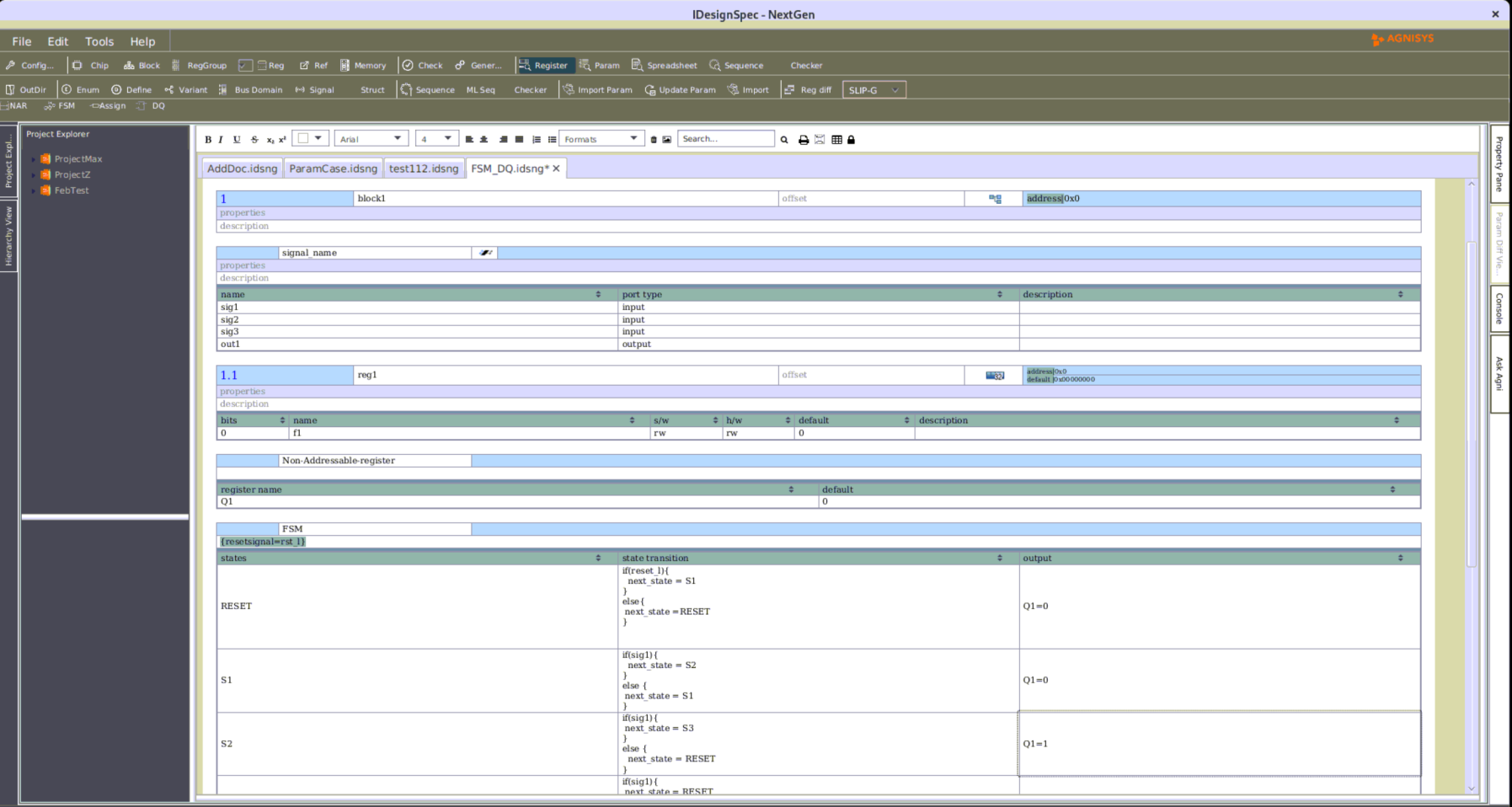
Templates, be they GUI or textual, can be used to describe state machines and datapaths. GUI-based templates help new users to easily get on board and visually understand the design intent. In contrast, textual templates are useful for version control and for working in a multi-user environment where diff and merge are required.
Irrespective of the format used, templates help the users capture high-level design intent in an intuitive manner. Templates provide the ability to describe higher level constructs with an automatic, tacit understanding of the semantics. Rather than explicitly describe the behavior, templates provide an implicit meaning to the high-level constructs. This reduces the need to write too much code and makes the specification more compact and less error prone.
The capability of this approach
- Integration of Hardware Design Elements: Streamlines the incorporation of Finite State Machines (FSMs), Datapaths, and Continuous Assignments into existing register-based specifications.
- Automated RTL and UVM Model Generation: Efficiently creates Register Transfer Level (RTL) and Universal Verification Methodology (UVM) Prediction models at the click of a button, including necessary glue logic.
- AI-Based UVM Testbench: Facilitates advanced AI-driven testing within a specially designed UVM testbench environment, aiming for 100% code and functional coverage.
- Edge Case Identification: The AI component in the UVM testbench excels at detecting and testing edge cases, ensuring comprehensive verification.
- Reduction of Manual Testing Effort: Significantly decreases the manual labor required in testing various inputs and in verifying the completeness of IP.
- Enhanced Test Accuracy and Speed: By automating testing processes, the tool not only speeds up the development cycle but also improves the reliability of the tests.
- Focus on Strategic Design and Verification: Reduces the time engineers spend on repetitive testing tasks, allowing them to concentrate on more critical aspects of design and verification.
The IDS-IPGen tool stands out for its comprehensive approach to integrating complex hardware design elements, generating essential models, and conducting in-depth AI-based testing to ensure thorough coverage and efficiency.
Example: SPI design
The diagram shows an SPI (Serial Peripheral Interface) communication scheme with one master device and three slave devices. The master controls the communication by sending a clock signal (SCLK) and selects which slave to communicate with using separate Slave Select lines (SS1, SS2, SS3). Data is sent from the master to the slaves using the MOSI line and received from the slaves on the MISO line. This setup allows the master to communicate with each slave individually or broadcast to all simultaneously, depending on the design.
SPI Block Diagram

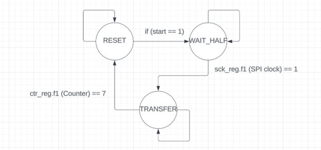
SPI FSM Design
The SPI design has a simple state machine at its heart. It is shown in the following diagram.

Output RTL Code
reg [2:0]FSM_Name_state;
if(start == 1) end if(sckreg_F1_q == 1) end if(ctrreg_F1_q == 7) end endcase // FSM_Name: Registered outputs, sequential always block sck_d <= 0; data_d <= data_in; end sck_d <= sckreg_F1_q + 1; sck_d <= 0; end sck_d <= sckreg_F1_q + 1; mosi_d <= datareg_F1_q; else if(sckreg_F1_q == 1) data_d <= (datareg_F1_q << 7) | miso; else if(sckreg_F1_q == 3) ctr_d <= ctrreg_F1_q + 1; data_out_d <= datareg_F1_q; |
Design Waveforms
This diagram illustrates the interaction between the SPI master and slave, highlighting the FSM state changes and the transmission of data from the SPI master to the slave, along with the MOSI and MISO signal dynamics.

UVM Prediction Model Code
begin end end end endcase begin if(!((rm.mosi_reg.F1.get()) == hw_if.mosi)) if(!((!rm.sck_reg.F1.get()) == hw_if.sck)) if(!((rm.data_out_reg.F1.get()) == hw_if.data_out)) if(!((rm.new_data_reg.F1.get()) == hw_if.new_data)) end |
Benefits of this approach
- Streamlined Verification:
- Minimize respins and optimize verification cycles
- Automated Test Generation:
- Generate UVM-based AI tests effortlessly with a single click from golden specifications
- Comprehensive Test Coverage:
- Cover all test scenarios comprehensively while automatically tracking code and function coverage
- Faster Verification:
- Reduce verification time, enabling engineers to be more efficient and productive
Summary
This article has shown the benefits of deploying a higher level specification to code generation approach that covers more than just addressable registers that can be described by SystemRDL or IP-XACT. This approach captures state machines and datapath and uses AI to then create Design and Verification collaterals thereby reducing the development time and simultaneously improving the quality at lower resource levels.
If you wish to try out Agnisys’ IDS-IPGen, please click here and then click on “Request an Evaluation”.


