Auto-Mirroring for Volatile Registers
Introduction
UVM Register Abstraction Layer (RAL) is a high-level object-oriented abstraction layer to access the registers in a design. The RAL model mimics the design registers and this allows the verification team to ensure correctness of the design. UVM RAL supports different register access like R/W, RO, WO, W1C, etc. from the CPU bus (we call it the software side). In addition, there is access from the application logic for which the design is being built (we call it the hardware side). The same model can be accessed by multiple software side buses. When a hardware event occurs in the design, the registers can be updated as a result. Such registers are called volatile registers. For example, a register can indicate the state of the application logic which is read by the CPU – hardware access is write-only, and software access is read-only. The value from the design (RTL) will not be mimicked on the RAL model on its own; something needs to be done. To overcome this shortcoming in the UVM RAL, we use a technique called auto-mirror. This article discusses how we handle it in IDesignSpec™.
How Hardware Can Be Updated in the UVM RAL Model
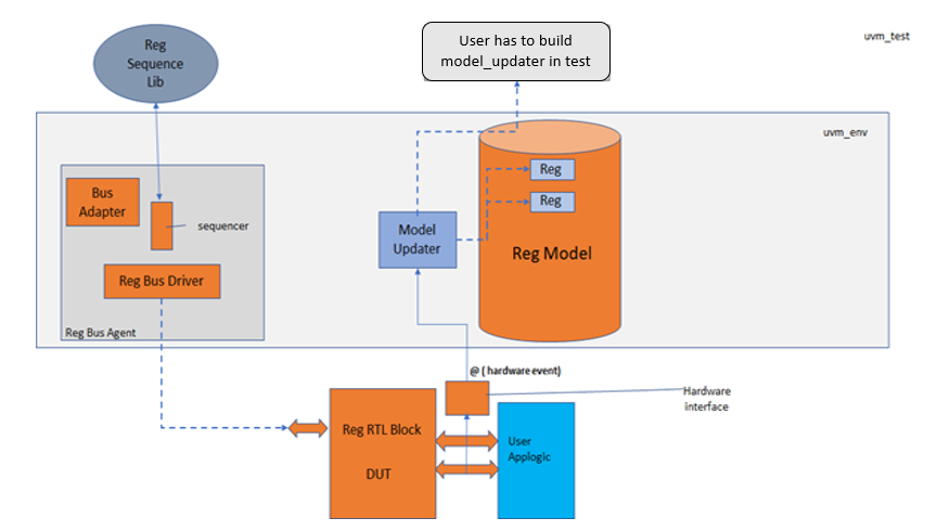
In auto-mirror, a task continuously monitors the hardware events occurring on the volatile registers through an interface (HW interface, i.e., a collection of hardware ports of all the volatile registers in the spec). Whenever a hardware event occurs, the field in the volatile register in the RAL model gets updated with the value on the HW interface.
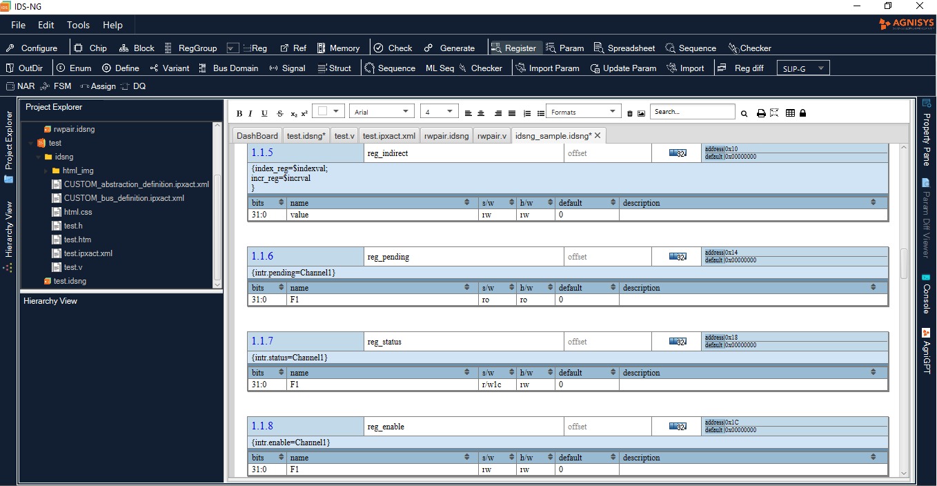
The feature of auto-mirror is enabled in IDesignSpec using the command line switch “-auto_mirror”.
In the diagram below, model_updater calls a task hw_update_mirrors, i.e., a collection of all volatile registers hw_update tasks.
In each individual task, a hardware event is being monitored and, when a hardware event occurs, it will update the value on that particular register in the register map.
Note: Auto-mirroring is currently supported at chip level.
Below are the files that are created while using “auto_mirror”:
<RAL_MODEL>.regmem.sv
Model_updater.svh
Hw_if.svh
HWif_access_block
In IDS we can also use auto-mirror for third-party RTL. Users just need to follow the below steps to integrate the auto-mirror in the UVM testbench.
Steps for integrating auto mirroring in the testbench:
1. Run the command:
idsbatch <inp_file> -out uvm -dir <out_dir> -auto_mirror
2. Build the model_updater class in UVM test. Here, add the model_updater.svh file in test_pkg.
3. Set UVM RAL model in the UVM test:
class Block1_test extends uvm_test;
` uvm_component_utils(Block1_test)
…
model_updater model_updater_h;
…
function void build_phase(uvm_phase phase);
super.build_phase(phase);
…
modelinst = Block1_block::type_id::create(“Block1”);
modelinst.build();
…
uvm_config_db #(Block1_block)::set(null, “uvm_test_top*”, “ral_model”, modelinst);
…
model_updater_h = model_updater::type_id::create(“model_updater_h”,this);
…
endfunction
endclass
4. Connect the register signals with the block_hw interface in module HWif_access_block.
module HW_intf_access_block;
import uvm_pkg::*;
Block1_hw_if Block1_hw();
/* Replace “User_RTL” on the right side with the hierarchical register port with HW_interface signal on left
example: assign Block1_hw.Reg1_F1_in_enb = wrapper.block1.Reg1_F1_LOAD;
assign Block1_hw.Reg1_F1_in = wrapper.block1.Reg1_F1_IN; */
//port connection for Reg1_F1
assign Block1_hw.Reg1_F1_in_enb = User_RTL.Reg1_F1_in_enb;
assign Block1_hw.Reg1_F1_in = User_RTL.Reg1_F1_in;
//port connection for Reg2_F2
assign Block1_hw.Reg2_F2_in_enb = User_RTL.Reg2_F2_in_enb;
assign Block1_hw.Reg2_F2_in = User_RTL.Reg2_F2_in;
initial
begin
uvm_config_db #(virtual Block1_hw_if)::set(null, “*”, “Block1_hif”,Block1_hw);
end
endmodule
Note: Replace the signals on the right-hand side of the assign statements with the hierarchical register signals of the DUT.
Block_hw.Reg1_F1_in_enb : HW enabling signal
Block_hw.Reg1_F1_in : Writing value of the register
5. Make an instance of HWif_access_block in top of UVM testbench
module top;
…
wrapper_block User_RTL(
.Block1_apb_if(Block1_ambaapb)
);
HW_intf_access_block inst();
…
endmodule
Note: Compile the HWif_access_block file before the top file.
6. Lastly, run the simulation
Conclusion:
Auto-mirroring enables the user to update the RAL model on the basis of hardware events occurring for each volatile register. This can be really helpful in special scenarios such as sampling the correct value in coverage in case of special registers like interrupt registers, and special register access.
Support for CDC Synchronization in IDesignSpec
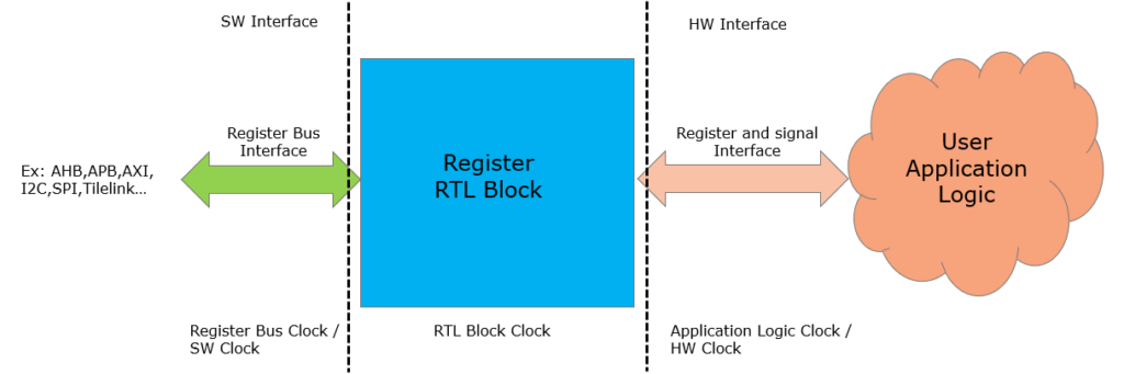
A typical SoC register block can be accessed from two sides. On one side, there is a register bus interface (we call it the software side) while on the other side, there are signals driven by the user’s application logic (we call it the hardware side). A register bus can be any industry standard parallel bus protocol like AMBA-AHB, AMBA-APB, AXI, Tilelink or serial buses like I2C or SPI. The register bus forms the SW interface while the signals driven from the user’s application logic form the HW interface.
In a multi-clock design, some or all three of these – SW interface, HW interface, and register block – are on different asynchronous clocks. Thus, the design can have the following three possible clock domains:
- Register bus clock domain
- Register block clock domain
- Application logic clock domain
Three Clock Domains in a Register RTL Block
As both data and control signals are transferred across these clock domains, proper synchronization techniques must be used to avoid metastability on them.
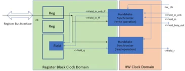
HW Interface Side CDC:
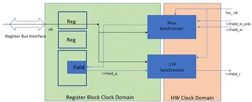
The register block HW interface consists of multiple data and control signals, which are used to perform read and write operations on any volatile register field in the block. IDesignSpecTM supports both simple mux synchronization and sophisticated handshake synchronization techniques to deal with metastability on the HW interface signals crossing the clock domain boundary.Mux Synchronization:
In this approach a mux synchronizer which is an open loop multi-cycle path formulation is used to synchronize the write data bus from the HW domain into the register block using write enable as the control signal.
The write data (<>Field_in) is directly registered into the register block domain without any synchronization, while the write enable control signal (<>Field_in_enb) is synchronized using a two-flip-flop synchronizer. Then, in the register block domain this synchronized write enable signal is used to load the write data onto the required flip-flop.
The read data (<>Field_r) is synchronized between the register block domain and the HW domain using a two-flip-flop synchronizer.
Below, a sample SystemRDL specification shows how the mux synchronization technique can be configured on the HW interface of a register field in IDesignSpecTM:
property cdc_clk {type = string; component = reg;}; [SystemRDL specification defining 2-FF and mux
synchronization technique for Reg1]
addrmap Block1{
reg Reg1{
cdc_clk = “hw_clk”;
field {}fld [0:0];
};
Reg1 Reg1;
};
Handshake Synchronization:
The mux synchronization approach works in design scenarios, where it is not required to sample each data value from the sending domain into the receiving domain.
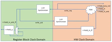
In designs where the sending clock frequency is greater than the receiving clock frequency, the sending domain data can change before it is synchronized into the receiving domain. Using a mux synchronizer in these designs can lead to data loss. A better approach is to use a handshake synchronizer, which is a closed-loop multi-cycle path formulation, on both read and write data paths.
During the write operation, as soon the write enable signal is asserted a write busy (<>Field_busy_out) flag is set. Then, this write enable control signal (<>Field_in_enb) is synchronized into the register block domain through a two-flip-flop synchronizer as write request. In the register block this synchronized write request is used to load the HW write data (<>Field_in) into the required flip-flop and an acknowledgement is send back to the HW domain.
An FSM in the HW domain controls the write busy flag, which is deasserted only when acknowledgement comes back from the register block. This enables the write data value to change only when the write busy signal is low and thus ensures that every data value is sampled in the register block
Write Operation
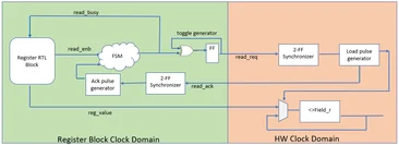
- Similarly, during the read cycle an FSM in the register block domain sets the read_busy flag on the read request. The toggle read request is then synchronized into the HW domain using a two-flip-flop synchronizer. The synchronized toggle is then converted into a load pulse on which the registered field data in the HW domain is fed into the HW read data bus (<>Field_r) and an acknowledgement is sent back, which deasserts the read_busy flag. As the field value can only be updated when the read_busy flag is low, no data loss occurs.
A sample SystemRDL specification below shows how handshake synchronization technique can be configured on the HW interface of a register field in IDesignSpecTM:
property cdc_clk {type = string; component = reg;}; [SystemRDL Specification defining Handshake synchronization technique for Reg1]
addrmap Block1{
reg Reg1{
cdc_clk = “hw_clk:handshake”;
field {}fld[31:0];
};
Reg1 Reg1;};
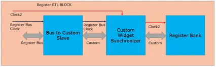
- SW interface side CDC:Certain design requirements may lead to having register block on a different clock than the bus clock. In this scenario an additional asynchronous input clock with respect to the bus clock is created on which read and write operations occur inside the register block.
First, the standard bus transactions are converted into a custom bus protocol, which is an internal IDesignSpecTM protocol. Both the register bus and the custom bus are on the same clock. Then the custom transactions are synchronized into the register block clock using handshake synchronization.
A sample SystemRDL specification below shows how the handshake synchronization technique can be configured on the SW interface of a register block in IDesignSpecTM:
property reg_clk {type = string; component = block;};
addrmap Block1{ [SystemRDL specification for placing Block1 on another
clock domain, “Clock2”, w.r.t the register bus]
reg_clk = “Clock2″;
reg Reg1{
field {}fld [0:0];
};
Reg1 Reg1;
};
Conclusion:
In a multi-clock-domain design, metastability is inevitable. However, by following critical design guidelines and using correct and well-established synchronization techniques, these expensive CDC failures can be avoided. IDesignSpecTM largely contributes in plugging these failures by automatically generating code that follows CDC design guidelines and allows users to configure different synchronization techniques according to their design requirements.
Difference between Paged & Alternate Registers
Introduction:
When creating a register map, sometimes designers need multiple definitions of a register as it appears to their logic. In IDesignSpec™ there are multiple ways to describe such registers, which can have multiple contexts. One possible way is to use paged registers, and another is to use alternate registers. In this article we will compare and contrast these two register types.
Paged Register:
A paged register is set of registers sharing the same physical address and a selector register used to decide which of them is accessed. A paged register in a design looks like:
- The top-level register map has an instance of the registers for a block and a “select” register.
- N instances of the register exist in hardware and, when a register is accessed, the access is directed to the right register based on the “select” register.
- Users can access a register in register-block X by using page-select to “select” instance X and then accessing the register in register-block X.
All registers will internally have N copies and a bit that selects which bank is written and which bank is used to output register values. Software should be able to toggle the select bit through a configuration register write.
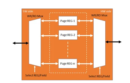
Figure (i): Representation of Paged Register
Users can also control the read and write of a paged register using two separate registers with the help of properties “page_rd_select = <reg_name>.<field_name>” and “page_wr_select = <reg_name>.<field_name>”
Alternate Registers
An alternate Register (also called a virtual register) consists of two or more registers at the same address location and, based on the execution mode, one register is selected. The selector can be a signal/register/register’s field.
Let’s take an example:
- Design has a 32-bit RW control register at block offset 4.
- In a default “run” execution mode (mode A), the register is interpreted as having 4 8-bit fields.
- In an alternate run execution mode (mode B), the counters are not being used so the same register is used by the DUT for a different purpose. In this case, the register is interpreted as two 16-bit fields.
- Users should also be able to write (software and hardware both) in one mode and read the value back in the other mode to see how the value will be viewed in the alternate mode.
- Randomizing and writing a value in a particular mode allows users to reference constraints and relevant fields based on that mode.
- Users should be able to display the register showing the fields based on a mode. The same for writing, reading, getting fields, randomizing, etc. – all should be based on the current mode that is applied to the regmodel.
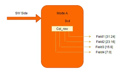
igure (ii): Representation of alternate register
Differences:
| Paged Register | Alternate Register |
| 1) In RTL, there are N internal storage i.e. equals to page count. There are N separate storage registers, all storing the same amount of data based on the context. | In RTL, there is only one physical storage for two or more registers. The number of modes defines how the storage is accessed. |
| 2) In IP-XACT, this can be achieved by adding additional information in <spirit:vendorExtension>. | In IP-XACT, alternate register can be defined using <spirit:alternateRegister> tags. It is used to have alternate views. |
| 3) Page register functionality is implemented using UVM callbacks in IDesignSpecTM. | In IDesignSpecTM, alternate register is supported using UVM standard class uvm_vreg. |
Summary:
IDesignSpecTM supports both paged register and alternate registers in RTL and UVM. The choice is based on what exactly needs to be accomplished. If the same entity is needed in different contexts, then a paged register is appropriate. If, however, there are two “views” of the same physical register then an alternate register can be used.
Smart Assembly of SoC Designs
System-on-chip (SoC) projects are, by their very nature, complex and difficult to complete successfully. Specification, architecture, design, and verification are all challenging. Increasing demand for design functionality and design performance makes every step of the design process more difficult, even the seemingly simple task of assembling all the pieces that make up the SoC.
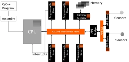
Today’s large chips may contain 500 or more instances of intellectual property (IP), a combination of new designs, reused blocks from previous projects, and licensed commercial IP. If each of these blocks averages 50 ports, then 25,000 connections must be made among them. Making these connections manually is tedious and time-consuming, with a high chance of errors. Meeting cost and schedule goals requires a big increase in the productivity of the SoC design team. Methodology improvements are needed to help accelerate assembly of chips and systems through automation.
Introduced in March, Agnisys SoC Enterprise™ is a flexible, customizable, and configurable IP and subsystem generator along with a tool to automate architectural level SoC assembly and connectivity. Its capabilities include:
- Fully compliant with the IP-XACT (IEEE 1685-2014) standard used by many IP providers to package their designs
- Creating and editing the design on-the-fly through scripts using text-based APIs and a GUI mode fully integrated within Agnisys IDS NextGen™ to view the resulting schematics for design analysis
- Generating major subsystems with flexibility to customize or configure
- Automatically adding instances to the design, making connections, restructuring, etc.
- Running design rule checks to ensure IP and SoC quality with facility for custom Design Rule Checks
Generating appropriate files for design, verification, and software teams
This Agnisys solution does more than assemble existing blocks; it can automatically generate the required “plumbing” blocks like aggregators, bridges, mirror-instances etc. Agnisys IDesignSpec™ generates RTL for registers and memories based on specifications. The SLIP-G™ library from Agnisys provides RTL generators for standard IP blocks such as GPIO, I2C Master, a timer, and a programmable interrupt controller (PIC) and many more. All of these are easily customizable and configurable to meet user requirements. SoC-Enterprise automatically integrates and connects all these blocks in the SoC using its AI based Smart Assembler technology.
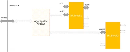
For standard buses such as AHB and APB, SoC-Enterprise can generate RTL aggregators, bridges, and multiplexors as needed to meet the required architecture for the SoC. For example, the AHB interfaces on two IP blocks can be aggregated into a single bus to connect to chip pins.
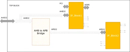
Similarly, if the design includes an IP block using AHB and IP blocks with APB interfaces, SoC Enterprise can automatically generate an AHB-to-APB bus bridge between the high-speed system bus and the lower-speed peripheral bus. Smart Assembler automatically integrates and connects these blocks as well.
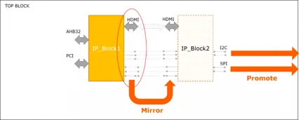
Smart Assembler can also automatically connect custom design blocks. The user can select a set of ports on a block and direct SoC Enterprise to automatically create the template for a new block with the same set of (mirrored) ports and then connect the two blocks. Smart Assembler can also connect existing blocks with mirrored ports and can even connect arbitrary blocks if the user provides a list of connections to be made. These capabilities provide a highly efficient way to populate the SoC with interconnected IP even before the RTL functionality is fully specified. The user can also have SoC Enterprise “promote” selected ports to the top level so that they can become chip pins.
Usages:
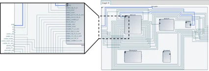
- In IDS NextGenTM, there is a console window displayed at the bottom of the IDS-NG tool that is used to display the verbose messages and error messages. This console window is also used for executing the SoC-Enterprise commands as shown in the image below:
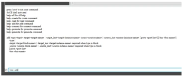
- SoC-E shell gets activated, then user can run not only the IDesignSpec Tcl commands but also SoC-E commands.
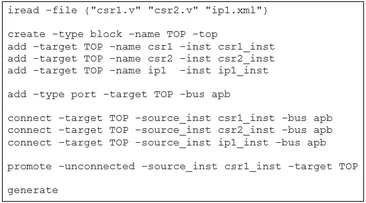
- Using a Tcl script: A Tcl script can be used to run SoC-Enterprise commands for instantiation, connection, design rule checks, and generation as shown in an example below.
Conclusion
The size and complexity of today’s SoCs demand automation for many aspects of design and verification. Chip assembly, including the connection of design blocks, is a prime target for increased designer efficiency and faster time to market. SoC-Enterprise provides an industry-leading solution. Effective IP and subsystem reuse is possible with the flexible, customizable, and configurable generators from Agnisys. SoC-Enterprise also supports reuse in verification, firmware, and software by generating appropriate files for those teams. Chip development is faster, better, and less expensive with this advanced automation.