
Every semiconductor project starts with a specification. Input from the product marketing team, the business development team, and current or potential customers identifies
a need in the market for a particular chip or IP block. Starting with a rough list of product features and attributes, over time a detailed specification is developed. System architects create the high-level design and define the hardware-software interface that the programmers will use to interact with the hardware. The major blocks in the design are defined and described.
The verification plan for this design is also developed, usually in a separate specification. There must also be a plan for how to validate the complete hardware-software system and how to test the fabricated device. Ultimately, most chips end up with multiple detailed specifications before a single bit of hardware is designed or a single line of code is written.
Traditionally, all these specifications are written in a natural language such as English using
a word-processing application. They exist online, but they are most certainly not executable
specifications that can be interpreted by software tools. Natural language is inherently
ambiguous and imprecise, not ideally suited for automation. In some specific domains, there is promising work to translate English descriptions automatically using artificial intelligence (AI) and machine learning (ML) techniques, and this paper will touch on this. However, the dream of having a completely executable chip specification in natural language is far in the future, or perhaps unachievable. Thus, the reality today is that specifications remain documents that must be read and interpreted by multiple teams on the project:
- Designers must create the register-transfer-level (RTL) hardware design
- Embedded programmers must write the device drivers, boot code, and firmware that
interacts with the hardware - Verification engineers must write the testbench, tests, and assertions used to verify that
the RTL design works as specified - Validation engineers must development a pre-silicon environment where the hardware
and software can be tested together as well as a strategy for final validation in the bringup lab - Technical writers must develop documentation suitable for end users.
Of course, different people interpret natural language differently. This leads to a lot of
redundant work on the project, as each team independently reads the specification and creates their required code and models from it. The verification and validation processes are designed to find bugs in the hardware and software, but unfortunately many of the test failures end up being due to inconsistent and divergent interpretations of a specification. A lot of time and effort is wasted trying to get everything and everyone in sync.
Perhaps the biggest problem is that this divergence happens repeatedly throughout the project, every time that a specification changes. The programmers might request additional hardware resources, the designers may find that some parts of the specification are impractical to implement in silicon, or a new feature may be required to respond to competition. As shown in Figure 1, every time, each team reads the updated specification and makes the required changes to their code or environment. This repeated effort by multiple teams leads to redundant work for everyone. It is challenging enough to keep all the teams in sync on the same version of an ever-changing document, but even when that works there is always the possibility of different interpretations of the changes in the specification. The resulting “waterfall effect” increases costs and delays TTM as each team deals with the specification changes.

Figure 1: Waterfall effect from each specification change
Overcoming the weaknesses in the traditional approach requires two improvements: writing the specifications in a precise format rather than natural language, and making this format executable so that electronic design automation (EDA) tools can generate as many files as possible for the design, verification, programming, validation, and documentation teams. Such a flow pays multiple dividends. Automation is always faster than manual effort, so many files are generated much more quickly and much less expensively than with traditional hand-coding. If the tools used for the generation are part of a unified suite of products, the issue of differing interpretation goes away completely. These benefits are repeated many times on the project. Every time that a specification is updated, it is automatically propagated to all teams and revised files are generated as needed. The dominos don’t fall, and the impact is minimal.
Agnisys is the industry leader in specification automation. For fifteen years, Agnisys products have read in executable specifications and generated a wide variety of files used by project teams. As noted earlier, technology today does not support an executable specification that can generate a complete SoC design at the push of a button, with the entire RTL description ready for implementation and all the embedded code ready to compile and run. However, Agnisys engineers realized that specifications for registers and memory could be fully automated, and over the years the company has added support for sequences, standard IP blocks, and chip-level interconnection. Figure 2 provides a concise view of the full Agnisys solution and Figure 3 shows the products in the Agnisys IDesignSpec™ (IDS) Suite. The following sections discuss the specific products and how they implement different parts of the overall solution.
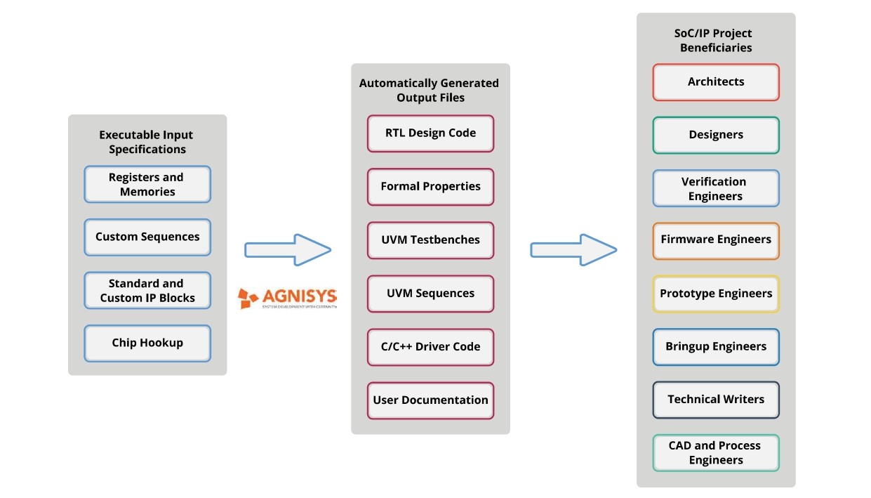
Figure 2: Full Scope of the Agnisys Solution Flow
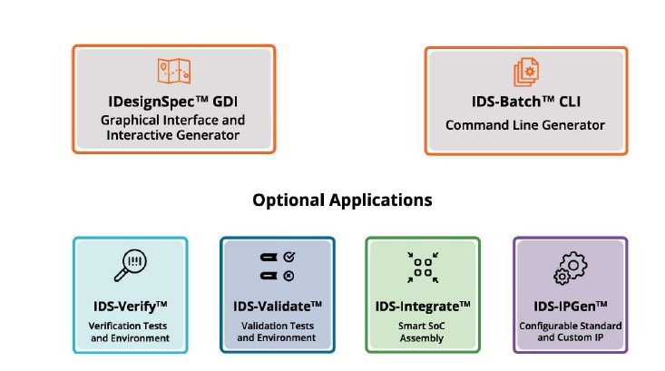 Figure 3: Summary of Agnisys IDesignSpec Suite
Complete the form to download your copy of this eBook.

The IDesignSpec Suite provides a complete solution for executable hierarchical specification of the memories, register sets, registers, and register fields in an IP or SoC. Users can choose from a variety of input formats. They can import existing descriptions in standard formats such as SystemRDL, IP-XACT, JSON, YAML, RALF, Custom XML and comma-separated values (CSV) files. Users can specify the registers and memories using Agnisys-supplied templates for Microsoft Word, Microsoft Excel, or OpenOffice Calc. For maximum benefit and flexibility, they can choose the highly intuitive specialized register and memory editor contained within the IDesignSpec GDI product, a graphical user interface (GUI) for specification entry. A smart editor for SystemVerilog and the Universal Verification Methodology (UVM) standard is also included in IDesignSpec GDI. This executable specification supports simple registers as well as more than 200 special register types, including indirect, indexed, read-only/write-only, alias, lock, shadow, FIFO, buffer, interrupt, counter, paged, virtual, external, read/write pairs, and combinations of these types. From the specifications, IDesignSpec GDI interactively generates output files for the design, verification, software, and documentation teams. It generates the complete RTL description for the registers and memories, including a bus slave and decode logic specific to the user-selected bus protocol and any clock-domain-crossing (CDC) synchronization logic needed. This enables instant connection of the user’s application logic to the register bus. Support interfaces include APB, AHB, AHB-Lite, AXI-Lite, AXI4, AXI4-Lite, TileLink, Avalon, Wishbone, AXI5, SPI, I2C and proprietary buses. The generated SystemVerilog, Verilog, VHDL, or SystemC RTL code for the registers is humanreadable with easy-to-follow comments. The hardware design team simply adds the generated files to their list of hand-written application logic RTL blocks and third-party IP blocks for use with simulation, logic synthesis, and other tools in the development flow. IDesignSpec GDI generates a SystemVerilog model compatible with the UVM standard and suitable for inclusion in a UVM testbench. This eliminates a lot of work on the part of the designers and the verification team. IDesignSpec GDI helps the embedded programmers as well, by generating C/C++ headers for the memories, registers, and fields. This replaces tedious manual transcription of specification details into code and avoids any chance of errors in the process.
For technical writers, IDesignSpec GDI generates high-quality documentation of registers and memories suitable for inclusion in user manuals. User-selectable formats include Microsoft Word, HTML, PDF, IP-XACT, and SystemRDL. The automatic generation of all these files ensures that the teams are always in sync and that all files are updated every time that the specification changes. Figure 4 shows all the formats for inputs and generated outputs supported for register and memory specification automation. The Agnisys IDS-Batch™ CLI product generates all the same files as IDesignSpec GDI, but in command-line mode. This is helpful when the IDesignSpec Suite is integrated into makefiles or check-in scripts for revision control systems. Whenever a specification changes, IDS-Batch CLI can be run automatically on the command line. Users can choose any combination of IDesignSpec GDI and IDS-Batch CLI licenses. All other Agnisys products also generate their outputs in command-line mode using IDS-Batch CLI and support graphical entry and interactive generation with IDesignSpec GDI, which serves as a unified GUI.
 Figure 4: IDesignSpec GDI Input and Output Formats for Registers and Memories
IDesignSpec GDI also includes special support for FPGA designers. Today’s programmable devices require many of the same development techniques and tools as ASIC and fullcustom designs, and the most sophisticated FPGAs fully qualify as SoCs. IDesignSpec GDI can use pre-defined IP blocks provided by FPGA vendors and generate scripts for use in their implementation tools. Both Xilinx and Intel technologies are supported.
While UVM testbench simulation is the primary method for verifying most SoC and IP designs, formal verification often plays an important and complementary role. Formal methods take assertion properties about the design and either prove that they hold true in all cases or generate counterexamples showing violations. This analysis considers all possible legal design behavior, so it frequently finds bugs missed in simulation. There is no way in simulation to ever prove that a design is correct, so formal verification also increases confidence in the design. IDS-Verify supports this powerful technique by enabling IDesignSpec GDI or IDSBatch to generate SystemVerilog Assertions (SVA) that run in all standard formal tools. The generated files include SVA assertions, SVA environmental constraints, SVA coverage metrics, SystemVerilog helper code, and makefiles. Running formal verification with design and these properties proves that all registers and memories conform to the specification. The generated assertions can also be run in simulation along with the UVM testbench. Figure 5 summarizes the support for simulation and formal provided by the IDesignSpec GDI family.
 Figure 5: Automatic Verification from Specifications with IDS-Verify
The register verification capabilities of IDS-Verify are extended to pre-silicon and post-silicon validation by the IDS-Validate™ product. IDS-Validate with IDesignSpec GDI or IDS-Batch CLI automatically generates both UVM and C/ C++ sequences, including specified custom sequences, that exhaustively test the memories and registers. IDS-Validate also extends beyond registers and memories to generate verification environments and user-defined functional tests to verify the functional behavior of custom design blocks. From a single specification using Python or Microsoft Excel, users can automatically generate tests that run in UVM and UVM-C hybrid environments, as shown in Figure 6, as well as physical boards. Thus, IDS-Validate covers both initial pre-silicon validation (also known as hardware software co-verification) and final post-silicon validation in the bring-up lab. Users can also generate output files for use in automated test equipment (ATE) programs.
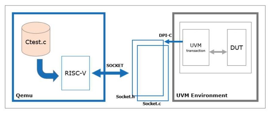 Figure 6: Example Hybrid UVM-C Verification Environment Generated by IDS-Validate and IDS-Batch CLI
The generated hybrid environments can run both C and UVM tests, coordinated by a
synchronizer component also generated by IDS-Validate. The environments are capable of
handling interrupts and their associated interrupt service routines (ISRs). Users can test the
connections between their design blocks and use the generated environment as a starting point for developing a complete SoC verification environment.
They can run the generated C/C++ code on their own embedded processors, or they can use a RISC-V SweRV Core EH1 packaged with IDS-Validate. Because the C/C++ programs are used to configure the design blocks, the configuration sequences can be used for testing as well as for software development. Embedded programmers can use the generated C/C++ code to develop and debug the SoC production software as well as device drivers. Figure 7 summarizes the inputs and outputs for IDS-Validate.
 Figure 7: Automatic Validation from Specifications with IDS-Validate
A typical SoC contains hundreds or thousands of RTL blocks from a variety of sources. Many
are hand-coded for the application logic, although the percentage of custom RTL has been
decreasing for many years as development teams take advantage of available IP blocks. Users of IDesignSpec GDI have all their register and memory blocks generated for them, ready for use in the design.
Many chip companies maintain in-house libraries for commonly used design structures and
interfaces. In addition, nearly all SoC projects also license IP blocks from partner companies or commercial IP providers, especially for blocks that implement a standard processor instruction set architecture (ISA) or interface protocol such as USB or PCI Express (PCIe). Leveraging IP and reusing parts of previous designs can save the SoC project team a huge amount of time and effort.
The downside of using fixed IP blocks is that the users may not be able to get exactly what they want. It is usually possible to modify and customize IP, but this is risky unless the designers have enough expertise in the ISA or protocol. Otherwise, they run the risk of breaking the standard functionality in the process of adding new functionality.
The best solution is to use IP generators rather than fixed IP blocks. Generators offer users
the ability to configure and customize many attributes of the IP design, including the options
defined by any relevant standards. These may include bus widths, number of ports, optional
functionality, power/performance/area (PPA) trade offs, and user extensions such as processor instructions beyond the ISA. The generator ensures that standards requirements are not compromised in the process of customization.
By taking advantage of specification automation, an IP generator can produce many output files to benefit the project teams. The Agnisys IDS-IPGen™ product is a powerful and flexible library of standard IP generators. Each library title uses IDesignSpec GDI or IDS-Batch CLI to generate a customized RTL design to meet the user’s requirements along with a UVM model, UVM tests, and matching documentation.
All these files reflect the customized aspects of the design, which the user specifies in the
IDesignSpec GDI unified GUI, as shown in the timer example in Figure 8. Some naysayers on using IP maintain that the verification and validation work for an unfamiliar design takes more time than just doing the design themselves. IDS-IPGen eliminates this objection because it handles all aspects of the IP block in every stage of development.
.jpg?width=755&height=363&name=Figure%208%20Example%20of%20User%20Customization%20in%20IDS-IPGen_page-0001%20(1).jpg) Figure 8: Example of User Customization in IDS-IPGen
Figure 8: Example of User Customization in IDS-IPGen
IDS-IPGen includes generators for numerous standard design blocks, including AES, DMA, GPIO, I2C, I2S, PIC, PWM, SPU, Timer, and UART. IDS-IPGen also supports the specification of custom IP blocks in the user’s application logic; users can specify finite state machines (FSMs), data paths, signals, and other relevant parts of the design. Figure 9 summarizes the IDS-IPGen flow and shows the files generated for standard and custom IP blocks.
 Figure 9: Automatic Generation from Specifications for IP Blocks
Hooking up hundreds or thousands of blocks into a top-level SoC design is conceptually easy,
but a tedious and error-prone process if done manually. Many similarly named signals must
be connected, with typographical errors highly likely. The step-and-repeat hookup of repeated instantiations of the same block is especially tedious. Detecting interconnection errors occurs rather late in the project, only when full-chip simulation is ready. Runs are slow and memory intensive at this level, and debug is challenging given the enormous size of the design.
Some EDA vendors have touted graphical hookup as an answer, but maintaining a schematic
with hundreds or thousands of blocks doesn’t really solve the problem. Even if the hookup
is done perfectly, the top-level design changes countless times during a project as the specifications change or design blocks are modified. Trying to track all these changes and keep the SoC consistent is a nightmare.
Agnisys has a solution to apply specification automation to SoClevel assembly and interconnection. The IDS-Integrate product provides a flexible and customizable environment to meet the design requirements for a complete chip. With IDesignSpec GDI or IDS-Batch CLI, it not only interconnects blocks, but also generates RTL components such as bus multiplexers, aggregators, bridges (AHB to APB, AXI to APB, and AXI4-Full to AHB-Full), and other “plumbing” components as needed. As expected, IDSIntegrate fully comprehends the register RTL designs generated by IDesignSpec GDI and the IP blocks generated by IDS-IPGen.
Users are not limited to designs generated by Agnisys. IDS-Integrate can handle any third-party IP block with an IP-XACT description and can even handle custom application logic blocks. The users can specify in Tcl or Python how their own blocks should be interconnected, including rules for intelligent name-mapping between block input and output ports with identical or similar names. As shown in Figure 10, IDS-Integrate assembles the complete top-level SoC based on this specification.
IDS-Integrate provides an automated, repeatable process that saves time and creates “correctby-construction” SoC designs. It eliminates manual coding errors when interconnecting RTL blocks. To help users check their specifications, it offers an intuitive graphical view of blocks and their connectivity with simple navigation through the chip hierarchy. Typical actions performed with IDS-Integrate include:
- Connecting an IDS-generated block with the user’s application logic and creating a
wrapper around it - Reading an IP-XACT component and connecting with the existing blocks
- Connecting an AHB bus with an APB slave by automatically instantiating a bridge
- Connecting several AHB blocks to an AHB master by automatically instantiating an
aggregator - Moving a block from inside a deep hierarchy several levels higher
 Figure 10: Automatic SoC Assembly from Specification
Many SoC and IP designs are used in safety-critical applications such as aerospace and defense, nuclear power plants, embedded medical devices, and self-driving cars. In all such uses, the designer must include safety mechanisms that will detect faults in the field and take appropriate action. Faults might be due to silicon aging effects, environment stress, or alpha particle hits; responses might include correcting the error, resetting the system, or bringing the system to a safe state. Many safety-critical applications have industry standards that set requirements for fault detection and recovery, and designers must comply in order to develop commercially viable products. The ISO 26262 standard for vehicles, including autonomous operation, is the best known. Others include IEC 61508 for industrial applications, IEC 61513 for nuclear plants, IEC 60601 for medical devices, and DO-254 for avionics.
Agnisys helps designers meet the requirements of these standards by automatically generating the safety logic to detect and report faults. Based on user specification, IDesignSpec GDI or IDSBatch CLI can generate the following types of safety logic included within the RTL design:
- Adding a parity bit to detect a changed value
- Calculating and checking a cyclic redundancy check (CRC) to detect a changed value
- Using single error correction double error detection (SECDED) to both detect and correct a
changed value - Implementing triple modular redundancy (TMR) so that two correct values will “outvote”
an incorrect value, as shown in Figure 11
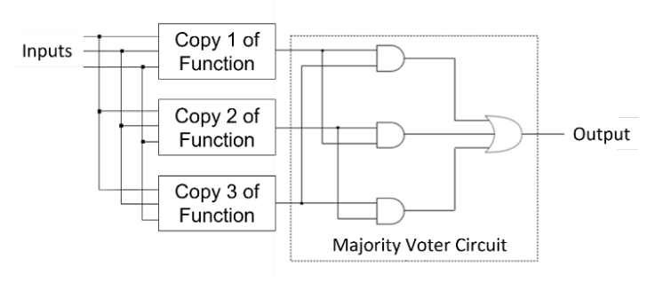 Figure 11: Triple Module Redundancy as a Safety Mechanism
Agnisys also helps with another key aspect of safety-critical design. Many safety standards
have strict requirements on how users document and certify their tools and flows they use for design and verification. ISO 26262, in particular, requires that the EDA tools used by automotive engineers must be qualified for use in developing functionally safe IP and chips. This can be a big effort that consumes significant extra cost and schedule delay while taking resources away from the main design and verification effort.
Fortunately for users, an EDA vendor can qualify its own tools as suitable for ISO 26262 design and have them certified by an independent testing organization. The Agnisys software products and development flow are certified by the internationally known testing and inspection organization TÜV SÜD as meeting the stringent tool qualification criteria defined by ISO 26262 and the related underlying functional safety standard IEC 61508.
Developers of automotive electronics can leverage the Agnisys IDesignSpec GDI Tool
Qualification Kit (TQK) to satisfy the demands of their customers who insist on standards
compliance. Users do not need to take any additional steps to qualify or certify the products
used in their flows, saving them significant time and money on their IP and chip projects.
Complete the form to download your copy of this eBook.